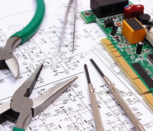
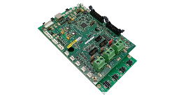
Professional Manufacturing
FR-4 PCB
FR-4: Brominated flame-retardant G-10 successor. Standard PCB epoxy laminate.
Request a Quote
What is FR-4 PCB?
Material Overview
An FR-4 PCB is a printed circuit board made from a widely used material known as FR-4, which stands for flame-retardant grade 4. The standard is defined by the NEMA, and it refers to a composite material made from woven fiberglass cloth combined with epoxy resin.
Key Benefits
FR-4 offers excellent mechanical strength, good thermal stability, and reliable electrical insulation. Its cost-effectiveness and wide availability make it the industry standard for the majority of PCB applications across consumer, industrial, and commercial sectors.
Precision Solutions
Benlida delivers precision PCB manufacturing with advanced equipment and strict quality control, ensuring consistent performance from single-layer boards to complex multilayer designs tailored to your specifications.
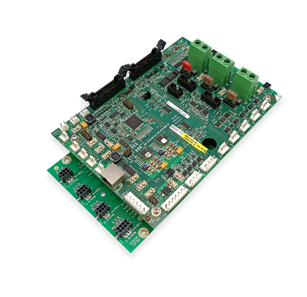
Our FR-4 PCB Manufacturing Capabilities
At Benlida, we deliver high-precision FR-4 PCB manufacturing with advanced technology, strict quality control, and fast, reliable production from prototype to volume.
Types of FR-4 PCBs
FR-4 PCB by Benlida: Durable, Affordable, and Built for Every Electronic Need.
Standard FR-4 PCB
Reliable and cost-effective, ideal for general electronic devices and everyday applications with high quality.
Get a QuoteHigh Tg FR-4 PCB
Designed for high-temperature environments, offering enhanced thermal stability and mechanical performance.
Get a QuoteHigh-Frequency FR-4 PCB
Optimized for fast signal transmission and reduced loss in RF and high-speed applications.
Get a QuoteMultilayer FR-4 PCB
Multiple layers enable compact, complex circuits for advanced electronics and high-density designs.
Get a QuoteHDI FR-4 PCB
High-density interconnect PCB for miniaturized devices with fine lines and microvias to match your demand.
Get a QuoteFR-4 PCB Manufacturing Process
Benlida FR-4 PCB: Expertly Crafted with Precision at Every Step, from Design and Lamination to Testing and Delivery.
PCB Design & DFM Review
Ensure optimal design and manufacturability before production to prevent errors and improve performance.
Material Preparation
Select and cut FR-4 substrate sheets to the required size and specifications.
Inner Layer Imaging
Transfer circuit patterns onto inner copper layers using photolithography for precise circuit definition.
Etching Process
Remove unwanted copper from inner layers to create the desired circuit patterns.
Layer Lamination
Bond multiple inner layers together under heat and pressure to form the multilayer board structure.
Drilling & Via Formation
Drill holes for component leads and electrical connections between PCB layers.
Copper Plating
Plate drilled holes and surface areas with copper to ensure electrical conductivity.
Solder Mask Application
Apply protective solder mask to prevent short circuits and protect traces.
Surface Finishing
Apply finishes like HASL or ENIG to protect copper and improve solderability.
Electrical Testing & Inspection
Test all circuits for continuity and defects to ensure quality and reliability.
FR-4 PCB Surface Finish
Benlida FR-4 PCB Surface Finishes: Perfect Protection, Superior Solderability, Every Time.
HASL
A traditional, cost-effective finish using molten solder, ideal for general-purpose PCBs.
Lead-Free HASL
Environmentally friendly version of HASL, meeting RoHS standards for lead-free electronics.
ENIG
Provides a flat, gold-coated surface for excellent solderability and reliable high-frequency performance.
Immersion Tin
Offers uniform, smooth surface with good solderability for short to medium-term applications.
Immersion Silver
Provides high conductivity and excellent surface planarity for precision assembly and fine-pitch parts.
OSP
Organic solderability preservative protects copper while remaining flat, perfect for fine-pitch components.
FR-4 PCB Design Guides
Benlida FR-4 PCB Stack-Up: Engineered for Precision, Signal Integrity, and High-Performance Designs.
FR-4 PCB design guidelines help engineers achieve reliable performance, stable signal transmission, and efficient manufacturability. By focusing on key design factors, it is possible to optimize both electrical and thermal performance.
Trace Width Considerations
Select appropriate trace widths to support current requirements and maintain controlled impedance.
Via Design
Optimize via size and structure to ensure reliable connections and minimize signal loss.
Thermal Management
Incorporate heat dissipation strategies such as copper pours and thermal vias to manage temperature effectively.
Layer Stack Planning
Design a well-structured stack-up to separate signal, power, and ground layers for improved stability.
Impedance Control Tips
Apply controlled impedance design to ensure consistent signal quality in high-speed circuits.
2-layer FR-4 stack-up
A basic configuration suitable for simple circuits with low component density and standard signal routing.
4-layer FR-4 stack-up
Provides additional layers for power and ground planes, improving signal performance and reducing EMI.
6-layer FR-4 stack-up
Offers more routing flexibility, better signal integrity, and supports complex high-speed designs.
Controlled impedance design
Ensures precise impedance values for high-frequency signals, critical in RF and high-speed digital circuits.
Signal integrity considerations
Optimizes layer arrangement, trace width, and spacing to minimize noise, crosstalk, and signal degradation.
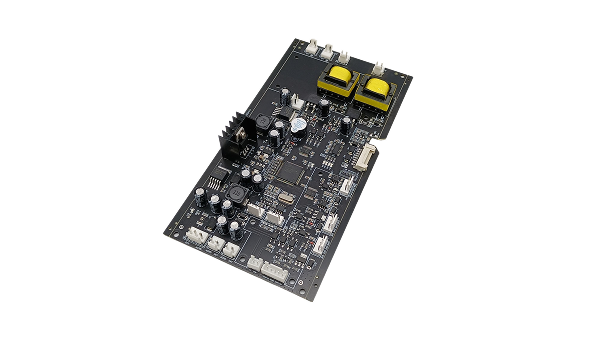
FR-4 vs Other PCB Materials
Step into our state-of-the-art manufacturing facility where precision meets efficiency. Every corner reflects our commitment to high-quality production, seamless workflow and strict quality control — delivering excellence in every PCB we build.
Why Choose Benlida for PCB Manufacturing?
Choose Benlida for precision PCB and PCBA manufacturing—delivering fast turnaround, consistent quality, and reliable performance from prototype to production.
Experienced Manufacturing
18 years of PCB manufacturing experience. Authoritative manufacturing team delivering consistent quality at every scale.
Request a Quote
Advanced Quality Control
Comprehensive inspection processes including AOI, X-ray, and functional testing ensure every board meets the highest standards.
Request a QuoteFast Turnaround
Flexible production schedules with rapid prototype delivery. From design to finished PCB in record time without compromising quality.
Request a QuoteGlobal Supply Chain
Trusted component sourcing from verified suppliers worldwide, ensuring authenticity and availability for every project.
Request a QuoteTurn Your Dreams Into Reality
Getting a custom PCB made is simple with Benlida. Submit your design files or project details, and our team will provide a fast, accurate quote tailored to your requirements. Whether it's a prototype or large-scale production, we make the process easy and efficient.