X-Ray Inspection in PCB Assembly — BGA and Hidden Joint Detection

What Is X-Ray Inspection in PCB Assembly?
X-ray PCB inspection can reveal hidden solder-joint defects beneath BGA, QFN, and other bottom-terminated components. It helps identify voids, bridges, missing solder, and misalignment that optical cameras cannot see. Detection depends on the imaging method and the defect. A clear image does not prove that every joint is sound.
Here, inspection concerns the assembled board, or PCBA, after soldering. It is different from testing an unpopulated PCB. X-rays pass through the assembly. The detector records how much the materials weaken the beam, known as attenuation. Solder and surrounding materials create contrast that helps locate internal features.
Systems may be manually operated or automated. AXI means automated X-ray inspection; it is not a name for every X-ray method. For broader production context, see our PCB X-ray inspection overview. This guide focuses on reading hidden-joint evidence and agreeing what counts as acceptable.
Why BGA and QFN Need X-Ray Inspection
In a ball grid array, the solder connections sit beneath the package body. Conventional AOI inspection can check visible placement features, but it cannot examine the complete hidden array. Our guide to BGA component packages explains the package structure.
Quad flat no-lead (QFN) packages also have underside connections, often including a central exposed pad. Some versions use wettable flanks to make external solder fillets visible to AOI. TI explains this wettable-flank design. Visible side fillets still do not show voids across the entire hidden pad.
These visibility limits make X-ray useful for hidden solder joint inspection. However, imaging and electrical testing answer different questions. A suspicious shape may need further investigation, while an apparently normal joint may still have an electrical problem.
Defects X-Ray Can Detect
Start with the component drawing, ball map, and PCB layout. Compare like-for-like joints and confirm the expected connections. An empty position may be intentional. A feature from the opposite board side may overlap the joint being inspected.
| Condition | Possible X-ray evidence | Interpretation limit |
|---|---|---|
| Voiding | Regions of lower attenuation within the solder image. | Measure against a defined area or volume. Location and overlap matter. |
| Solder bridging | Solder appears to connect neighboring joints. | Confirm that the apparent connection is not an overlapping feature. |
| Missing or insufficient solder | An absent ball or an unusually small or irregular solder image. | Check the intended ball pattern. Shape alone does not quantify every connection. |
| Misalignment | Joint features are offset from their intended pads. | Interpret the image using the package geometry and viewing angle. |
| Suspected head-in-pillow or open joint | An abnormal interface, separation, or joint shape may be visible. | Top-down 2D can miss the condition. Additional views or analysis may be needed. |
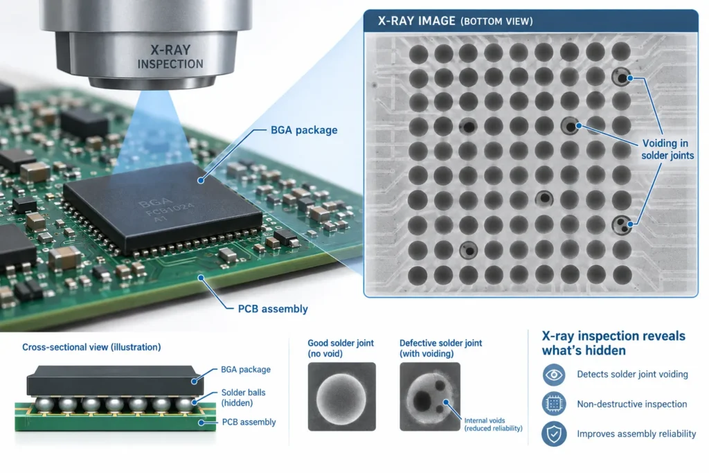
Infineon’s BGA assembly recommendations describe X-ray detection of bridges, voids, and other soldering problems. They also warn that broken solder joints are not always easy to detect.
Head-in-pillow occurs when a BGA ball and the reflowed solder paste fail to form a proper metallurgical bond. They can appear to touch. An IPC-hosted study of head-in-pillow detection shows why image appearance can be misleading. Treat uncertain findings as unresolved, not automatically passed. Suitable 3D imaging or destructive failure analysis may help clarify them.
2D vs 3D X-Ray (CT) Inspection
2D X-ray produces a projection through the assembly. Structures at different depths appear in the same image. It can screen BGA arrays for obvious bridges and voids when the relevant features are distinguishable. Oblique views change the viewing angle, but they remain projections.
3D methods reconstruct information from multiple views. CT produces a volume that can be examined in slices. For flat assemblies, computed laminography or planar CT may provide useful views of selected solder interfaces. These methods have different acquisition geometries and reconstruction limits.
Comet Yxlon’s explanation of computed laminography shows how virtual sections help examine joints obscured by opposite-side features. This is useful when a 2D image cannot separate the target joint from its background.
Do not assume 3D inspection is always an offline, slow process. Nordson’s inline AXI systems combine several imaging modes. Choose the method by the defect and required evidence. Ask whether the proposed scan can resolve the interface of concern on your actual assembly.
Acceptable Voiding Levels
There is no single void percentage that should be copied across every BGA and QFN application. IPC-A-610 covers electronic assembly acceptability. The official IPC revision table lists IPC-A-610J, issued in March 2024. Use the revision and product class agreed for the order, with the applicable package and customer requirements.
Read the relevant clauses in the full standard. A revision list is not a source for a numeric acceptance limit. BGA solder balls and QFN exposed pads have different structures and functions. A requirement for one must not automatically become the acceptance rule for the other.
For example, TI’s QFN and SON attachment guide discusses exposed-pad voiding in a thermal-design context. Such guidance needs to be checked against the exact device and application. It is not a universal BGA acceptance rule.
For a projected-area report, the basic calculation is detected void area divided by the defined joint area, multiplied by 100. Record what the denominator represents. A 2D area percentage is not a 3D volume percentage. Voids at different depths can overlap in projection.
Before using an X-ray voiding inspection result for acceptance, agree on:
- The package, joint type, and applicable acceptance document.
- The measurement method, joint boundary, and image-analysis settings.
- Whether total voiding, the largest void, or a particular interface must be evaluated.
- The review process for borderline images and disagreements.
A low reported percentage does not clear a separate bridge, open joint, or non-wetting concern. Review these conditions independently.
When X-Ray Inspection Is Recommended vs Optional
Consider BGA X-ray inspection during first-article builds, process changes, and investigation of intermittent failures. Reworked hidden joints also deserve a defined verification plan. The decision should follow the actual package risks and customer requirements.
Routine X-ray may be optional for some assemblies with accessible joints and a validated inspection and test plan. For hidden joints, agree whether inspection covers every board, selected components, or a defined sample. Never reduce required coverage simply because a previous sample passed.
A useful inspection record identifies the board revision, unit or lot, component reference, and joint location. Include the image or slice, measurement basis, acceptance reference, result, and action taken for suspect joints. Ask the assembler what records the quotation includes.
Inspecting every board does not mean detecting every possible defect. Retain the agreed electrical and functional tests. For sensitive components, also ask the device supplier and inspection provider about permitted X-ray exposure.
FAQ
Why can’t AOI inspect BGA solder joints?
AOI needs an optical view of the feature. The BGA body hides most solder connections, so cameras cannot inspect the complete array. Side views may show some outer joints. X-ray provides information about concealed features, while electrical tests assess different aspects of the connection.
What voiding percentage is acceptable in BGA solder joints?
Use the applicable standard revision, product class, package guidance, and agreed customer criteria. Do not copy one percentage across all BGA and QFN joints. Confirm whether the report measures projected area, a selected slice, or volume before comparing the result with a limit.
What is the difference between 2D and 3D X-ray inspection?
2D combines features along the beam path into a projection. 3D methods reconstruct depth information and allow examination of slices or volumes. They can help separate overlapping structures. Neither approach guarantees detection of every defect; resolution and the inspection setup still matter.
Is X-ray inspection standard on all PCB assembly orders?
No. Coverage depends on the agreed order and inspection plan. Specify the components, sampling or full-board coverage, acceptance criteria, and required records. Ask the assembler to confirm these items before production instead of assuming X-ray is automatically included.
Define X-Ray Inspection Requirements with Benlida
For a project-specific discussion of PCB quality control, identify the PCBA’s BGA and QFN components and the hidden joints of concern. Send Gerber or ODB++ files, the BOM, pick-and-place data, assembly drawing, quantity, and revision. Add your inspection criteria and electrical or functional test requirements.
Ask Benlida to confirm the available imaging method, coverage, reporting, and quotation scope for your assembly. If CT or a specific void measurement is required, state it explicitly so feasibility can be reviewed.

