

Professional Rigid-Flex PCB Manufacturing
Rigid Flex PCB Supplier
Benlida provides custom rigid-flex PCB and flex-rigid PCB solutions with precision manufacturing capabilities, delivering reliable PCB products from prototypes to high-volume production for various industries.
Cost-effective for moderate complexity designs
Balanced cost and functionality
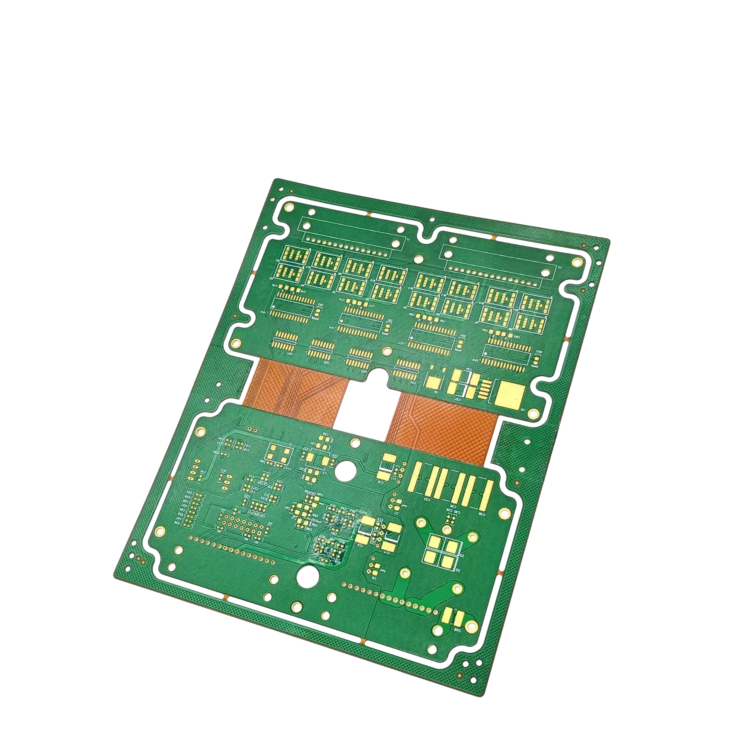
What is Rigid-Flex PCB?
Overview
Rigid Flex PCB is a kind of printed circuit board where rigid and flexible circuit technologies have been integrated in one board. Rigid sections are made using ordinary PCB material such as FR4, whereas the flexible sections are made using bendable materials such as polyimide. At the same time, being an experienced rigid flex pcb supplier, we can offer you customized rigid flex PCB solutions for your projects.
Advantages
Our solutions help you save space and weight when you compare them with separate rigid and flexible boards. The use of our solutions helps you reduce the number of connectors and cables, which increases reliability and durability. Our solutions are perfect for projects with a high level of performance.
Applications
Rigid-flex PCB technology is widely used in compact electronic devices such as smartphones, wearables, and medical equipment. It is also suitable for high-density or 3D configurations where space is limited, providing flexible design options and reliable electrical connections.
Related services and board types: Explore our PCB Manufacturing Services or compare Flexible PCB options.
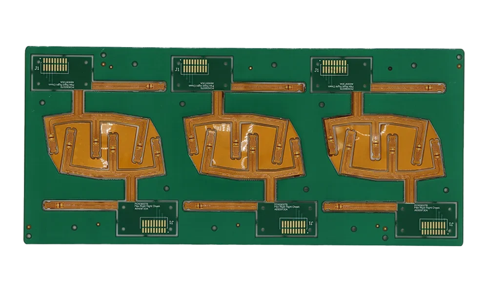
Our Rigid-Flex PCB Manufacturing Capabilities
At Benlida, we support rigid-flex PCB production with 1–16 layer capabilities, fine line processing, controlled impedance, and multiple surface finish options to meet different design requirements. As an experienced rigid flex PCB supplier, we provide reliable flex-rigid PCB solutions with precise manufacturing standards, supporting both prototype development and volume production.
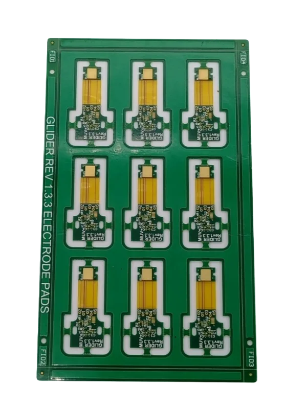
Layer Count
1-16 layers
Impedance Tolerance
±10% (+5Ω if <50Ω)
Min Board Size
3×3 mm
Inner Copper Thickness
1-2 oz (up to 4.5 oz for 2-layer)
Surface Finish
HASL, Lead-free HASL, ENIG
Hole Tolerance
Plated: +0.13/-0.08 mm; Non-plated: ±0.2 mm
Min Plated Slot
0.5 mm
Min BGA Pad
0.25 mm
Controlled Impedance
Supported (4-16 layers)
Max Board Size
Up to 670 × 600 mm
Outer Copper Thickness
1-2 oz (up to 4.5 oz for 2-layer)
Gold Finger Bevel
Supported
Min Via Size
0.15 mm (hole) /0.25 mm (pad)
Min Track Width/Spacing
0.10/0.10 mm (standard)
Min Non-Plated Slot
1.0 mm
Backdrill
Supported (up to 16 layers)
Rigid-flex PCB Manufacturing Process
Our rigid-flex PCB production follows a complete manufacturing process, including DFM review, material preparation, layer lamination, surface finishing, and electrical testing to ensure consistent quality and reliability. As a trusted rigid flex PCB supplier, we provide customized flex-rigid PCB solutions with strict process control from initial design review to final inspection.
1
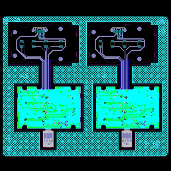
Rigid-Flex Design Review & Engineering Planning
Our engineers evaluate the rigid-flex PCB design, layer structure, bending requirements, and application environment to develop an optimized manufacturing solution.
2
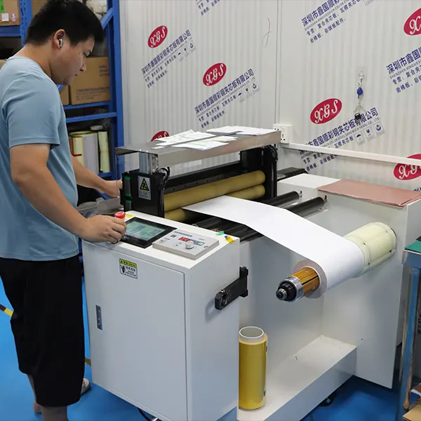
Flexible Circuit Material Preparation
Flexible materials such as polyimide films and copper foils are selected and prepared according to electrical, mechanical, and durability requirements.
3
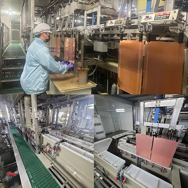
Flexible Layer Circuit Fabrication
Precision imaging and etching processes are used to create flexible circuit patterns, ensuring accurate traces and reliable performance in bending areas.
4
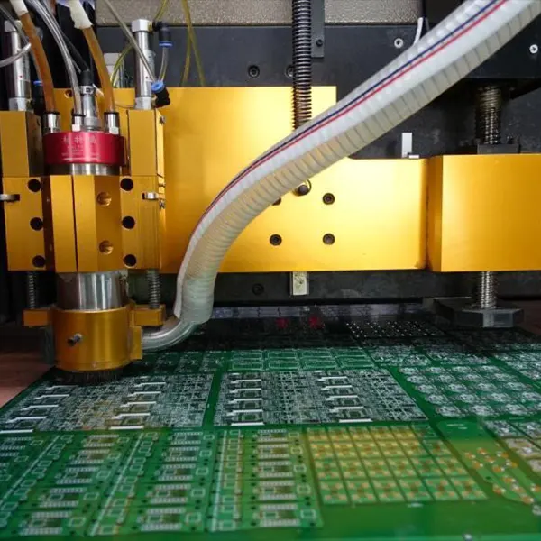
Rigid Section Manufacturing
Rigid PCB sections are fabricated using controlled processes to provide mechanical support and accommodate component mounting requirements.
5
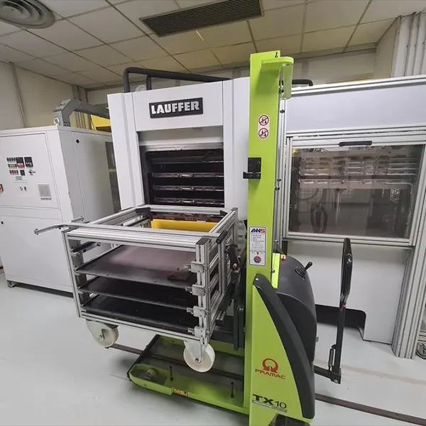
Rigid-Flex Layer Alignment & Lamination
Rigid and flexible layers are precisely aligned and laminated together under controlled pressure and temperature to form an integrated rigid-flex structure.
6
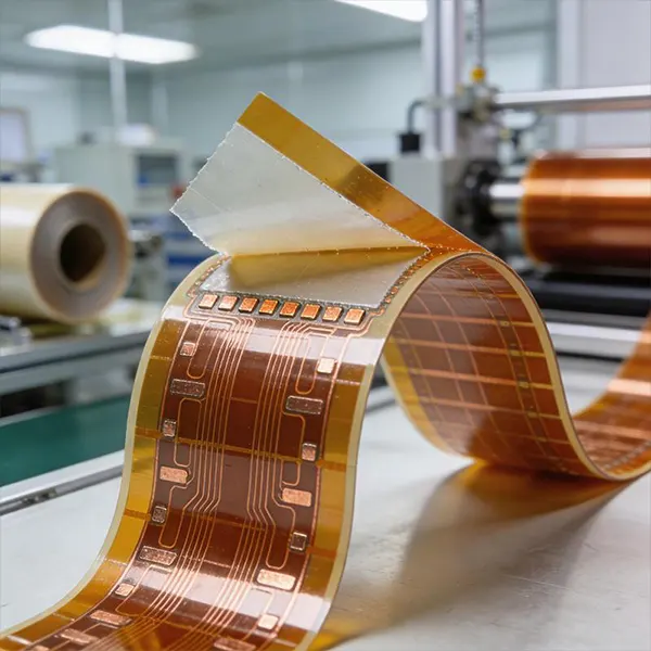
Coverlay, Stiffener & Protection Application
Coverlay films, stiffeners, and protective materials are applied to enhance insulation, mechanical strength, and bending reliability in flexible areas.
7
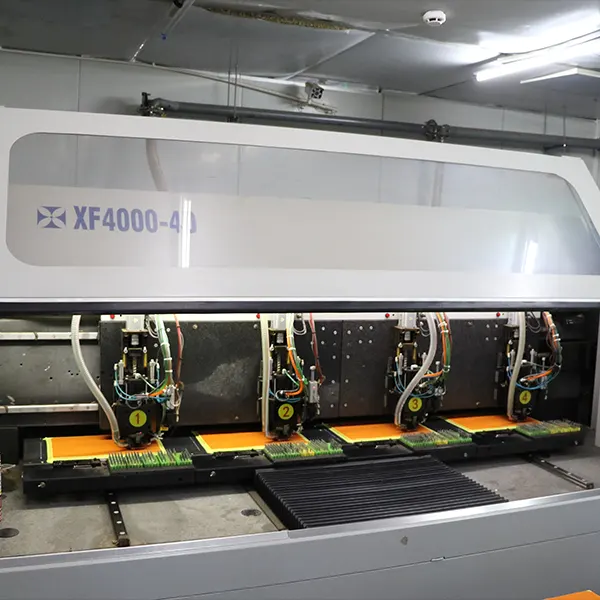
Drilling, Plating & Electrical Interconnection
Precision drilling and copper plating processes create reliable connections between rigid and flexible sections while maintaining signal integrity.
8
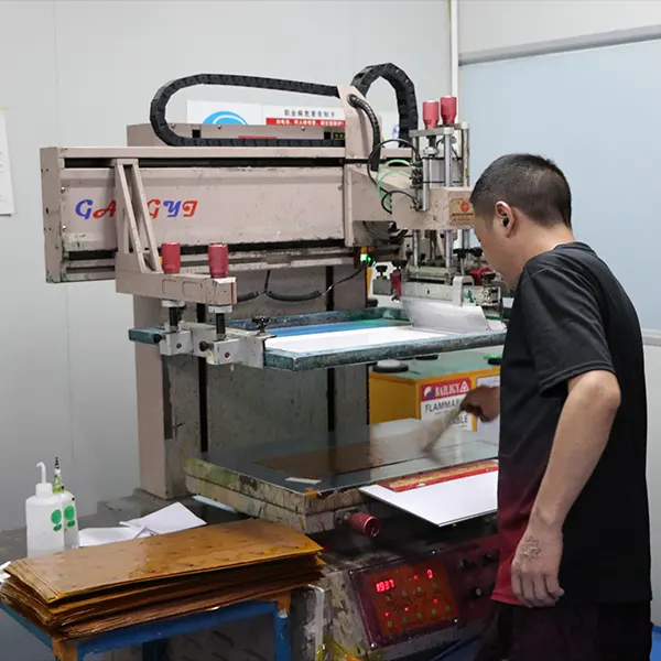
Surface Finishing & Final PCB Processing
Surface finishes, solder mask, silkscreen printing, and profile processing are completed to prepare the rigid-flex PCB for assembly.
9
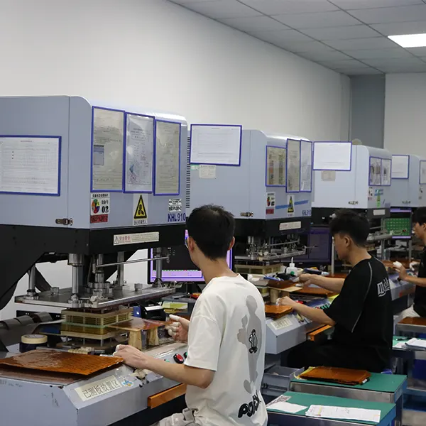
Reliability Testing & Quality Inspection
Rigid-flex PCBs undergo electrical testing, dimensional inspection, visual checks, and flexibility testing to verify product quality and long-term reliability.
10
Packaging & Delivery Preparation
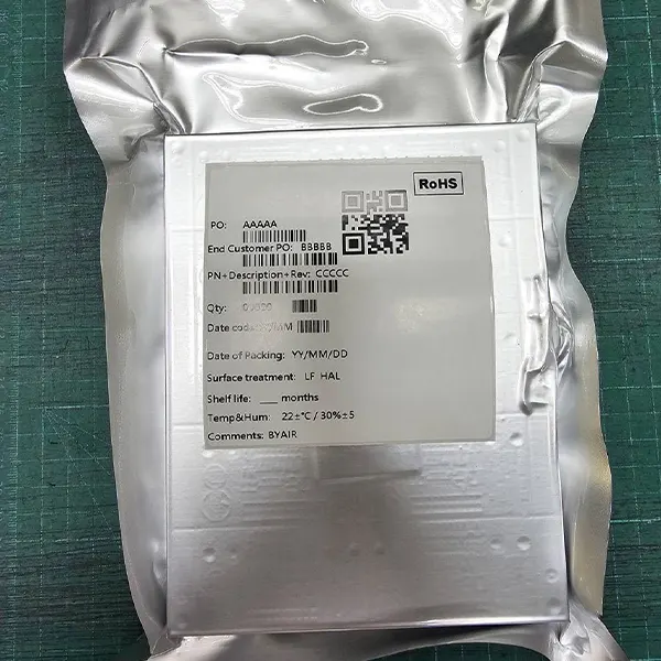
Finished rigid-flex PCBs are carefully packaged with protective materials, labeled according to customer requirements, and prepared for safe and reliable delivery.
Why Choose Benlida?
Meet Complex Design Requirements
Rigid-flex PCB designs often require higher integration and precision. Benlida helps customers achieve compact and reliable solutions by combining rigid and flexible circuit technologies into one optimized board structure.
Support Customized Applications
From consumer electronics and medical devices to high-density electronic systems, we work with customers to develop suitable flex-rigid PCB solutions based on different application requirements, space limitations, and performance needs.
Ensure Stable Quality and Performance
Our controlled manufacturing process, including DFM analysis, AOI testing, electrical testing, and quality control, can guarantee the same performance of the PCB from prototype to mass production.
Reliable Support from Development to Production
As a flexible rigid PCB manufacturer, Benlida offers full technical support for customers from design evaluation and prototype fabrication to mass production in order to minimize the risk during development and enhance manufacturing efficiency.
Rigid-flex PCB Design Guides
Rigid-flex PCB technology is commonly employed in small-scale electronic gadgets, including smartphones, wearable devices, and biomedical equipment. Moreover, this technology can be applied in high-density designs or 3D designs where there is not much space available.
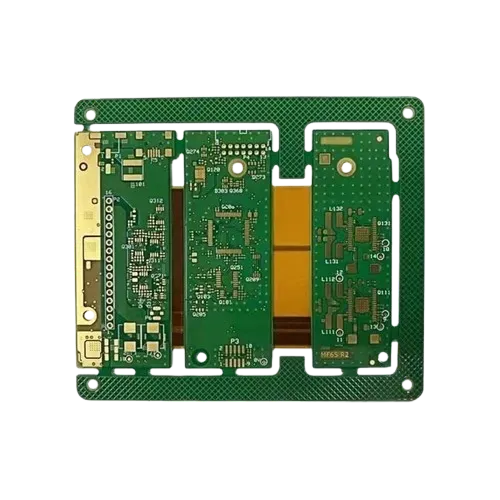
Designing a rigid-flex PCB requires careful planning to balance flexibility, durability, and electrical performance. Key guidelines include:
Optimize Bend Areas
Plan flex regions with an appropriate bend radius to reduce stress and prevent circuit damage during repeated folding or motion. Proper bend area design is essential for achieving reliable performance in flex-rigid PCB structures.
Layer Stackup Design
Rigid and flexible layers should be arranged separately in a strategic manner to preserve their performance parameters and avoid damage.
Trace Routing
Use consistent trace widths, avoid sharp corners, and minimize vias in flex areas to maintain reliability and stable electrical performance.
Component Placement
Place components on rigid sections whenever possible and avoid positioning heavy or high-stress components on flexible areas to improve durability.
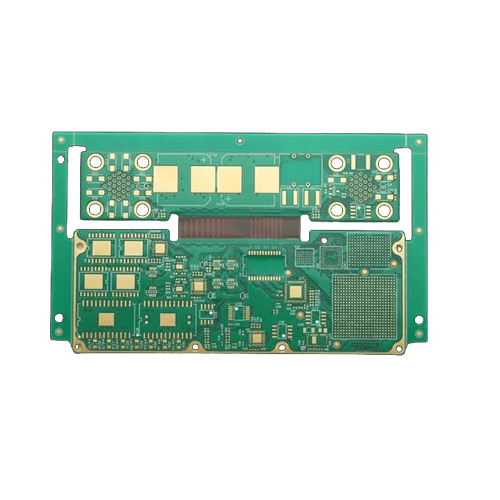
Designing a rigid-flex PCB requires careful planning to balance flexibility, durability, and electrical performance. Key guidelines include:
Mechanical Support
Stiffeners should be applied to the areas that can be subjected to excessive bending and thus ensure protection from failure.
Thermal Management
Proper calculation and distribution of copper layers is essential to keep the board cool and functional.
Design for Manufacturability
It is important to make sure that traces, vias, and pad sizes comply with the production capacity. It would help to collaborate with a professional rigid flex PCB manufacturer for better results.
Turn Your Dreams Into Reality
Getting a custom PCB made is simple with Benlida. Submit your design files or project details, and our team will provide a fast, accurate quote tailored to your requirements. Whether it’s a prototype or large-scale production, we make the process easy and efficient.
Key Features of Rigid-Flex PCB
Space-Saving Design
Rigid-flex PCB consists of rigid boards and flexible circuits integrated into one PCB, eliminating connectors and cables and providing more space in small electronic devices.
Lightweight and Compact Structure
Combining many circuit connections in one PCB, rigid-flex PCB makes devices lighter and helps to develop thinner products.
Enhanced Reliability
There are fewer connectors and solder joints in this type of PCB, which guarantees reliable connections and increases the durability of the PCB in any environment.
Flexible 3D Design Capability
The flexible sections allow the PCB to be bent or folded according to product requirements, making it suitable for complex three-dimensional and space-limited designs.
Improved Mechanical Durability
The advantage of rigid-flex PCB is that it provides improved resistance to vibration, movement, and mechanical forces in comparison with conventional PCB assemblies.
Wide Application Compatibility
Rigid-flex PCB assembly technology is used for the production of medical instruments, portable electronics, consumer goods, and many other products where reliability and flexibility of the design are needed.
Rigid-Flex PCB Testing and Inspection
To ensure the reliability and performance of each rigid-flex PCB, we perform extensive tests and inspections during the manufacturing process. They assist in confirming electrical performance, manufacturing precision, and reliability before shipment.
Automated Optical Inspection (AOI)
AOI technology is used for identifying any faults in circuits, such as open circuits, shorts, and any other faults, to ensure proper circuitry construction.
Electrical Testing
Electrical tests are conducted to test the continuity of the circuits, insulation efficiency, and signaling capabilities to help ensure stability of the final product.
Impedance Testing
Controlled impedance test ensures that high-speed signal needs are met in accordance with design specifications.
X-Ray Inspection
An X-ray test is utilized to examine internal structures, vias, and hidden connections within a multi-layer flex rigid PCB design.
Dimensional and Visual Inspection
Finished boards are inspected for dimensions, surface quality, solder mask, and surface finish to ensure they meet customer requirements.
Quality Verification Before Shipment
Final inspection and verification are completed before shipment to ensure each rigid flex PCB supplier project meets required quality standards and production specifications.
Industries Using Rigid-Flex PCB Solutions
With the use of rigid-flex PCB technology, industries requiring efficient and durable circuit designs can rely on this product as a solution to their needs. The combination of both rigid and flexible circuit designs makes it possible for rigid-flex PCBs to enable customers to make good use of their spaces, simplify their assembly processes, and provide products with reliable performance.
Consumer Electronics
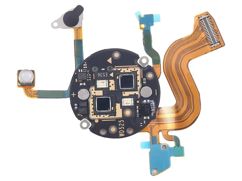
Through the application of rigid-flex PCB technology, thin, light, and compact electronic devices like smartphones, wearables, and portable devices become possible with the proper utilization of internal spaces and a smaller number of connectors.
Medical Devices
Medical equipment requires high reliability and precise circuit integration. Rigid-flex PCB supports compact designs and stable performance for diagnostic devices, monitoring equipment, and other medical applications.
Automotive Electronics
In automotive systems, rigid-flex PCB offers great durability and vibration resistance, thus is ideal for electronic modules and applications that need to operate in harsh conditions.
Aerospace and Industrial Equipment
The use of Rigid Flex PCB will help enhance design flexibility as well as wire simplification for aerospace and industrial applications where there are issues with space restrictions and mechanical stability.
High-Density Electronic Applications
In cases where there are complicated designs or restricted installation space for products, a flex-rigid PCB is an effective solution.
FAQ
Our rigid-flex PCB manufacturing capability supports 1–32 layers, allowing flexible configurations for different circuit complexity and application requirements. By means of proper stack-up design and manufacturing process optimization, we provide reliable performance of high-density electronic designs for our clients.
The rigid-flex PCB is an assembly of rigid materials like FR-4 and flexible materials like polyimide to create one integral circuit board. The material is selected according to the flexibility, mechanical strength, signal performance, and environmental conditions of application.
Yes. Controlled impedance is available for rigid-flex PCB designs, helping maintain signal integrity for applications with high-speed or sensitive electronic requirements. Proper stackup planning and trace design are essential to achieve stable electrical performance.
Rigid-flex PCB can be made using various surface finishes such as HASL, lead-free HASL, and ENIG. The right one can be chosen depending on soldering, component suitability, and application requirements.
Flex-rigid printed circuit board (PCB) design involves several important factors to be considered in order to ensure effective and successful PCB design. Proper planning contributes to higher reliability and manufacturing efficiency.
Yes. As a rigid flex PCB supplier, Benlida supports projects from design review and prototype production to volume manufacturing, helping customers achieve consistent quality and reliable delivery for different application requirements.
Core Structural Types of Rigid-Flex PCB
There exist various types of rigid-flex PCB structures depending on the layer structure, flexibility needs, and design complexity. Choosing the appropriate structure contributes to efficient use of the available space, as well as to enhanced performance of the PCBs in terms of electrical conductivity and mechanical stability.
Conventional Rigid-Flex PCB Structure
The traditional rigid-flex PCB includes rigid sections of boards together with flexible circuits using a normal layered structure. Such a structure is characterized by its compromise between mechanical and flexibility characteristics.
Multilayer Flexible Circuit Structure
The structure of a multilayer flexible circuit has several layers of flex circuits, which provide an option for more complicated routing and denser circuitry. Increased design flexibility is achieved in this way, and such a structure is mostly applied in projects that involve lightweight construction, three-dimensional designs, or limited space for mounting.
Advanced Asymmetrical Stackup Structure
The advanced structure of an asymmetrical stackup consists of having different layer configurations or different materials on both sides of the PCB, and this structure gives additional design flexibility for complex rigid-flex PCBs with certain electrical or space requirements.
Rigid-Flex PCB with HDI Technology
HDI technology, when combined with the rigid-flex PCB, gives the benefits of fine lines, small vias, and high component density. It is ideal for electronic products that need miniaturization.
High-Quality Materials Ensuring Long Flexing Life
The bend reliability of a rigid-flex PCB depends mainly upon the material used, stack-up design, and manufacturing process. Benlida uses dependable materials in the rigid and flexible layers, thus making the rigid-flex PCB extremely flexible and mechanically strong, along with reliable electrical performance.
Polyimide (PI) Flexible Material
Polyimide is chosen for use in flexible layers of flex-rigid PCBs owing to its flexible nature, heat resistance, and mechanical strength that allow the circuit to cope with bending stress while retaining its electrical performance.
High-Performance FR-4 Material
The use of FR-4 in rigid layers provides mechanical support and strength. The use of FR-4 and flexible materials allows rigid-flex PCBs to be both rigid and flexible.
Rolled Annealed (RA) Copper
RA copper is preferred for flexible circuit areas because of its superior ductility and fatigue resistance. It helps improve bending performance and reduces the risk of copper cracking during repeated flexing.
Adhesive Materials and Coverlay
High-quality adhesives and coverlay materials are used to protect flexible circuits, enhance insulation performance, and improve overall durability in different operating environments.