
Professional PCB Manufacturing Services & Custom PCB Boards
PCB Manufacturing Services
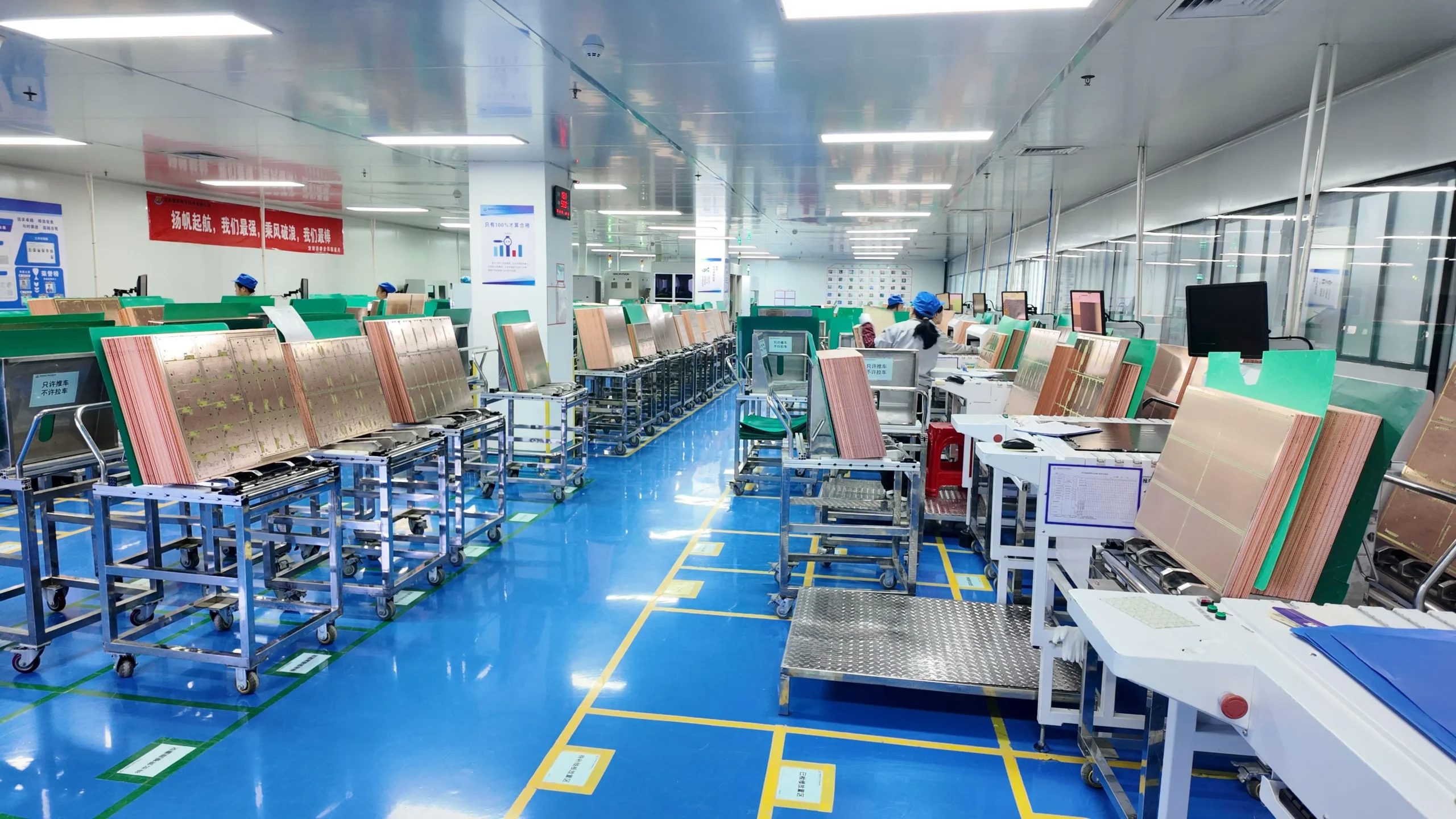
Benlida provides professional PCB board services with advanced manufacturing capabilities, supporting high-precision PCB fabrication, complex designs, and customized solutions for various industries.
Prepare Your Bare PCB RFQ
For a bare PCB quote, provide the available fabrication data and project requirements below. Make sure all files belong to the same design revision, and mark any item that is still open for review.
- Fabrication data: Gerber or ODB++ in the format agreed for the quote, plus NC Drill data when it is separate.
- Fabrication drawing: Board outline, dimensions, cutouts, slots, hole details, and critical mechanical tolerances, as applicable.
- Board construction: PCB type, layer count, stack-up, material, and finished board thickness.
- Copper and finish: Finished copper weight for each layer, surface finish, solder mask, and silkscreen requirements.
- Quantity and delivery format: Quote quantity, individual boards or panels, and panelization requirements when applicable.
- Controlled requirements: Impedance targets and tolerances, critical dimensional tolerances, and any special via or process requirements.
- Inspection and test: Required bare-board electrical testing, impedance verification, reports, or other acceptance criteria.
- Revision: Current fabrication-data revision and applicable change notes.
PCB Manufacturing Capabilities
Use this table for initial PCB project screening. The listed capabilities apply only under the stated conditions. Final manufacturability depends on the complete design, material, stack-up, copper weight, tolerances, surface finish, quantity, and test requirements.
| Capability | Range and Conditions |
|---|---|
| Layer Count | 1–32 layers. |
| Minimum Track / Spacing | 0.075/0.075 mm (3/3 mil) at 1 oz. |
| Mechanical Drill / Finished Hole | Minimum mechanical drill: 0.20 mm standard; 0.15 mm by engineering review. Minimum finished hole: 0.20 mm. |
| Laser Microvia | Minimum laser microvia: 0.10 mm, subject to HDI stack-up and engineering review. |
| Finished Board Thickness | 0.4–3.2 mm standard; other thicknesses are subject to stack-up and engineering review. |
| Finished Copper Weight | Outer: 1–4 oz standard, up to 8 oz by review. Inner: 0.5–2 oz standard, up to 4 oz by review. |
| Maximum Board Dimensions | Up to 600 × 1200 mm for rigid FR-4; larger formats are subject to material, layer-count, thickness, and process review. |
| Through-Hole Aspect Ratio | 8:1 standard; up to 10:1 subject to engineering review. |
| Controlled-Impedance Tolerance | ±10% standard; tighter tolerances down to ±5% are subject to stack-up, material, and verification review. |
| Outline Tolerance | CNC routing: ±0.10 mm; V-scoring: ±0.50 mm. Tighter tolerances require review. |
| Hole / Thickness Tolerances | PTH: +0.13/-0.08 mm; NPTH: ±0.05 mm. Board thickness: ±10% at ≥1.0 mm and ±0.10 mm below 1.0 mm. |
| Materials | FR-4, aluminum-core, and copper-core. High-Tg, halogen-free, Rogers/PTFE, flex, rigid-flex, and HDI constructions require project review. |
| Surface Finishes | HASL (leaded and lead-free), ENIG, and OSP. Hard gold, immersion silver, immersion tin, and ENEPIG require project review. |
Multilayer PCB Manufacturing
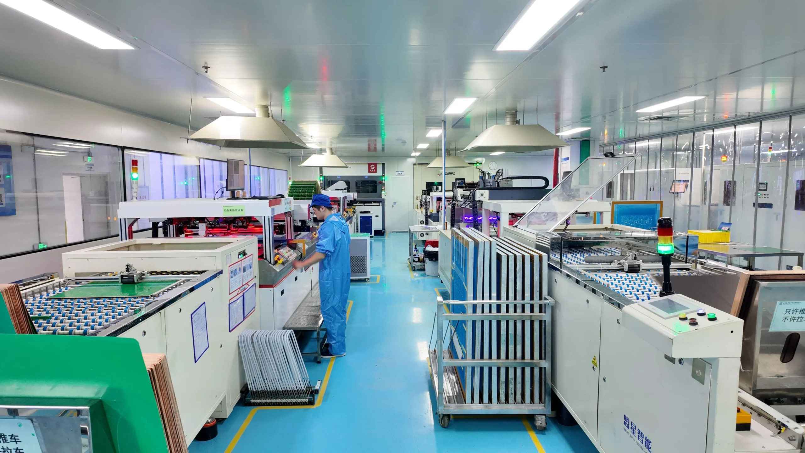
Benlida supports multilayer PCB production for complex circuit designs that require higher routing density and improved electrical performance. Multilayer structures enable more compact designs while maintaining signal integrity and reliability.
HDI PCB Manufacturing
Our HDI PCB capability supports high-density circuit designs with finer traces and advanced interconnection structures. It is suitable for compact electronic devices that require higher integration and efficient space utilization.
High-Frequency PCB Manufacturing
We offer high-frequency PCB board manufacturing solutions for applications where signal transmission needs to be constant and electrically controllable.These PCBs are designed to meet the demands of high-speed communication and RF-related applications.
Special Structure PCB Manufacturing
Benlida manufactures various special structure boards, including rigid-flex PCB and flexible PCB (FPC), offering greater design flexibility for products with limited space or complex mechanical requirements.
Heavy Copper PCB Manufacturing
The high-current copper printed circuit boards allow us to use the technology in applications that demand a greater current-carrying capacity and better thermal performance.
Drilling, Plating and Via Requirements
Hole sizes, via structures, plating requirements, tolerances, and any filled or capped via requirements should be identified in the released fabrication data. Feasibility and applicable conditions depend on the complete board construction and agreed order requirements.
Final Bare-Board Verification
Final verification for an unpopulated PCB should be defined by the released manufacturing data and order requirements. Applicable checks may cover workmanship, dimensions, continuity, and isolation. Methods, coverage, acceptance criteria, and required records should be confirmed for the project.
PCB Manufacturing: From Design Data to a Finished Bare PCB
PCB manufacturing converts released design data into an unpopulated circuit board that matches the project’s electrical, mechanical, and material requirements. The fabricator builds the physical board defined by the approved manufacturing package. Component installation is a separate PCB assembly process.
A complete manufacturing package must give one consistent definition of the board. Fabrication data, drill data, the board drawing, the stack-up, and project notes should agree. Any conflict should be resolved before production because it can change the physical construction or acceptance criteria.
The output is a finished bare PCB ready for inspection and project-defined electrical verification. It does not confirm the function of the final electronic product. Component sourcing, placement, soldering, programming, and functional testing belong to the PCBA scope and require separate production and acceptance information.
PCB Types We Serve
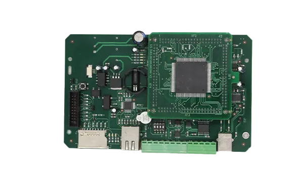
Benlida provides comprehensive PCB manufacturing services covering a wide range of PCB types, from standard FR-4 boards to advanced HDI, high-frequency, and specialty PCBs. With advanced manufacturing capabilities and professional expertise, our PCB board service delivers reliable, high-performance, and customized solutions to meet the needs of various electronic applications.
FR-4 PCB
Standard fiberglass PCB offering reliable performance, cost-effectiveness, and wide use in general electronics.
Multilayer PCB
Multiple copper layers enable complex circuits, high density routing, and improved electrical performance with high quality.
HDI PCB
High-density design using microvias and fine traces for compact, high-performance electronic devices to match.
Ceramic PCB
Excellent thermal conductivity and stability for high-temperature, high-power, and high-reliability applications.
High-Frequency PCB
Uses low-loss materials and controlled impedance structures for RF, microwave, and high-speed signal applications.
Heavy Copper PCB
Uses thicker copper conductors to support higher current, thermal management, and demanding power electronics applications.
Rigid-Flex PCB
Combines rigid and flexible sections for compact design and improved mechanical reliability.
Flexible PCB
Bendable circuits ideal for compact, lightweight, and dynamic electronic applications.
LED PCB
Optimized for heat dissipation to enhance LED performance, lifespan, and energy efficiency.
Custom PCB
Supports project-specific materials, stack-ups, dimensions, surface finishes, and design requirements after engineering review.
PCB Manufacturing Process
Input: The review uses the current-revision fabrication data in the format agreed for the project, such as Gerber or ODB++ data, plus separate NC Drill data when applicable, the fabrication drawing, and the specified stack-up, material, board thickness, copper weight, surface finish, impedance, tolerances, and other special fabrication requirements.
DFM review before fabrication: For an applicable PCB project, Benlida reviews the submitted fabrication package and agreed order requirements for manufacturability against the applicable process limits. Depending on the project and the data supplied, the review may cover file consistency, layer structure, copper features and clearances, holes and vias, board outline or panelization, solder mask, surface finish, impedance, and specified tolerances.
Output and customer confirmation: If information is unclear or a manufacturing change needs approval, the customer receives an engineering query identifying the point to resolve and the decision required. Fabrication proceeds from the customer-released revision and agreed requirements after required questions are resolved.
Scope boundary: This DFM review evaluates manufacturability only. It does not validate electrical design intent or finished-product functionality, and it is not a zero-defect guarantee. For questions before ordering, contact Benlida about PCB DFM.
Design Review & DFM Check
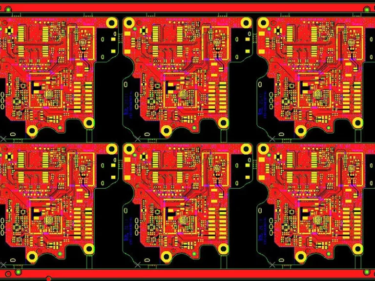
Engineers review the PCB design files and perform a DFM (Design for Manufacturability) analysis to verify circuit layout, layer structure, and manufacturing feasibility before production.
1
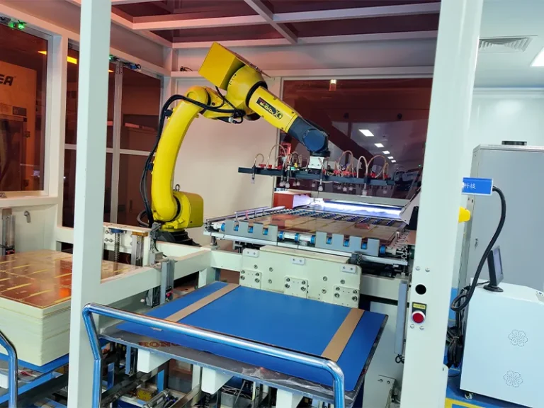
Material Preparation & Inner Layer Fabrication
High-quality copper-clad laminates are prepared according to PCB requirements. For multilayer PCBs, inner circuit patterns are created through imaging and etching processes.
2
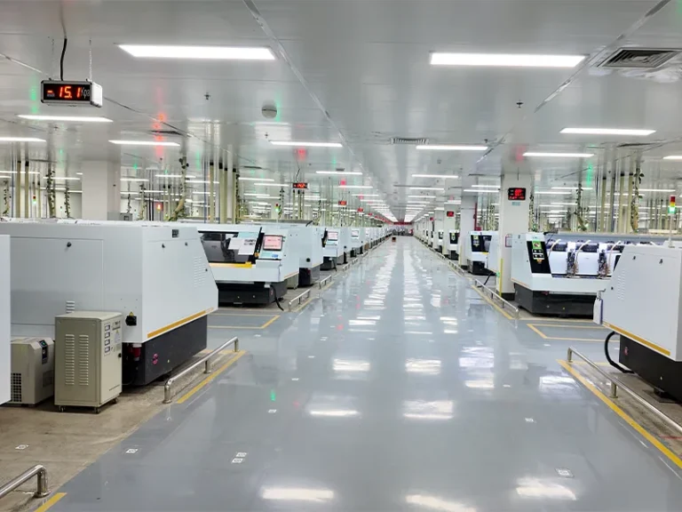
Lamination & Drilling
Multiple PCB layers are aligned and laminated under controlled temperature and pressure. Precision drilling is then performed to create holes for electrical connections and component mounting.
3
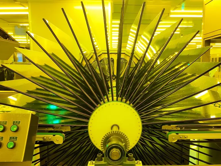
Copper Plating & Circuit Formation
The drilled holes are plated with copper to establish connections between layers. Additional etching processes are used to form the required circuit patterns.
4
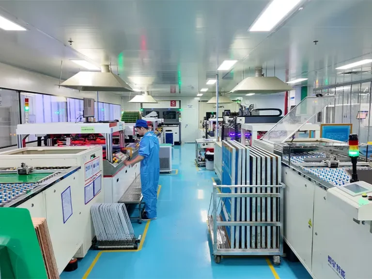
Solder Mask & Surface Finishing
A solder mask is applied to protect the circuits, followed by surface finishing treatments such as ENIG, HASL, or OSP to improve durability and solderability.
5
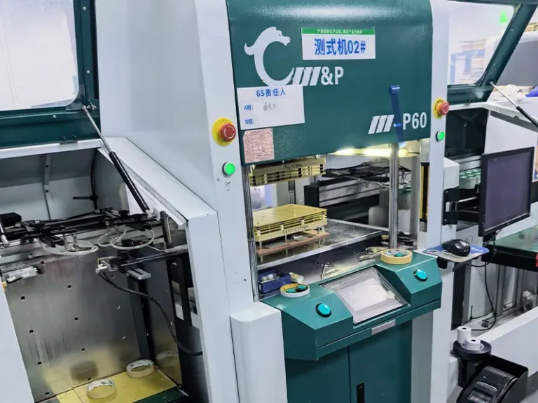
Inspection & Electrical Testing
Finished PCBs undergo strict quality inspections and electrical testing to ensure circuit integrity, reliability, and compliance with customer requirements before delivery.
6
Bare PCB Inspection and Electrical Testing
Inspection and test requirements for bare PCBs should be defined before production. The plan depends on the approved fabrication data, board construction, acceptance criteria, and customer requirements. The checks below apply only to unpopulated boards, and the method, coverage, and required records should be confirmed for the order. View PCB Testing & Quality Control.
Visual and AOI Inspection
Visual inspection checks workmanship and visible surface conditions. During fabrication, AOI compares circuit patterns with the approved data to identify potential opens, shorts, nicks, and excess copper. The inspection stage and acceptance criteria must follow the project specification.
Dimensional and Workmanship Inspection
Board outline, hole locations, board thickness, solder mask, legend, and surface finish can be checked against the fabrication drawing and agreed acceptance criteria. The measured characteristics and inspection frequency depend on the project specification.
Bare-Board Electrical Testing
Netlist-based electrical testing checks continuity and isolation on a finished bare board. It can identify opens and unintended connections, but it does not validate the function of an assembled product. The method, limits, coverage, and acceptance criteria must be agreed for the order.
Electrical Test Method Selection
Common bare-board electrical test methods include flying-probe and dedicated-fixture systems. Method selection depends on board design, probe access, order quantity, tooling, and required coverage. The applicable method must be confirmed during quotation review.
Controlled-Impedance Verification
For controlled-impedance designs, provide the target impedance, tolerance, stack-up constraints, and coupon requirements with the fabrication data. The verification method, sampling plan, and report format should be agreed before production.
Test Documentation When Required
For projects that require inspection or electrical test records, specify the required data, report format, traceability details, and acceptance criteria in the purchase requirements. Available documentation and report content should be confirmed before production.
PCB Customization Capabilities
PCB manufacturing options may vary by board type, construction, material, and fabrication process. The applicable options should be defined in the released fabrication data and confirmed for the order.
PCB Types Customization
Benlida supports a wide range of PCB types based on different application needs, including FR-4 PCB, multilayer PCB, HDI PCB, high-frequency PCB, heavy copper PCB, rigid-flex PCB, FPC, and LED PCB. These options allow customers to select the right PCB solution for their product requirements.
PCB Structure Customization
We provide customized PCB structures according to design requirements, including multilayer structures, high-density interconnect designs, and rigid-flex configurations. This helps meet the needs of complex circuit layouts and different product designs.
Material Selection
Different PCB materials can be selected based on application requirements, including FR-4, high-frequency materials, and ceramic materials. Material selection helps ensure the PCB meets the required performance and application conditions.
Manufacturing Process Customization
According to customer design files and production requirements, Benlida provides customized manufacturing processes, including circuit patterning, drilling, plating, solder mask application, and surface finishing. These processes ensure the finished PCB meets the specified design standards.
Surface Finish and Marking Requirements
Specify the required surface finish, solder mask, legend, marking, and related appearance or acceptance requirements in the fabrication data. The applicable options should be confirmed for the board construction and order scope.
Panelization and Delivery Format
Define whether boards are required as individual units or panels, together with the outline, routing or scoring requirements, tooling features, and project-specific handling notes. Feasibility should be confirmed from the complete fabrication data.
For PCBA requests: PCB assembly is a separate service. For an assembly quote, also provide a BOM, Pick-and-Place/Centroid data, assembly drawings, and any programming or functional test requirements. View PCB Assembly Services.
Why Choose Benlida?
This page focuses on bare PCB manufacturing. Project suitability depends on the released fabrication data, board construction, fabrication requirements, inspection criteria, and agreed order scope.
Complete PCB Manufacturing Capabilities
Benlida supports a wide range of PCB products, including FR-4 PCB, multilayer PCB, HDI PCB, high-frequency PCB, heavy copper PCB, rigid-flex PCB, FPC, and LED PCB. This allows us to provide suitable PCB solutions for different electronic applications.
Professional Engineering Support
Before production, our engineering team reviews customer design files and performs DFM checks to evaluate manufacturability. This helps identify potential issues early, optimize the production process, and reduce manufacturing risks.
Flexible PCB Customization Solutions
Project requirements may vary by PCB type, structure, material, and fabrication process. The applicable options should be reviewed against the released fabrication data and agreed order requirements.
Support from Prototype to Mass Production
Benlida provides PCB production support from prototype projects to larger-scale manufacturing. This flexibility allows customers to choose suitable production methods according to different project stages and requirements.
Support for Different PCB Applications
With diverse PCB manufacturing capabilities and flexible production processes, Benlida supports various electronic applications, including high-density, high-frequency, and specialized PCB requirements.
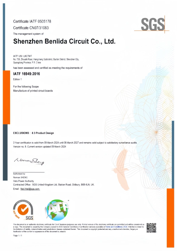
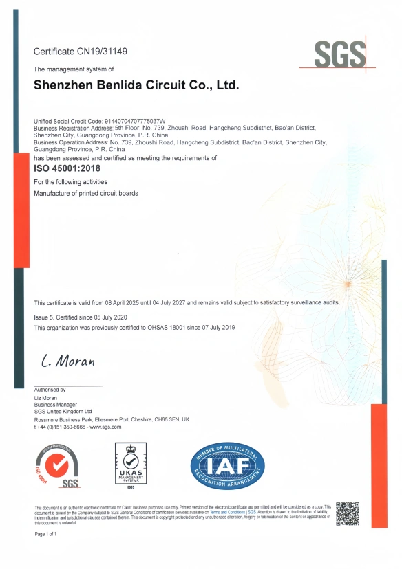
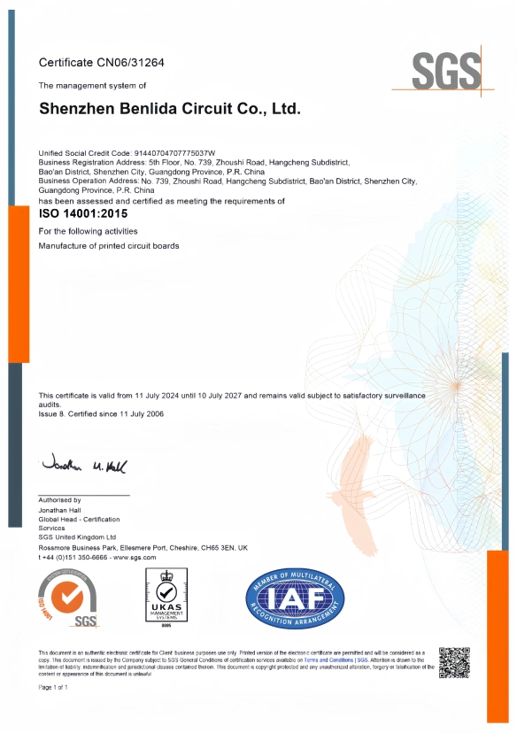
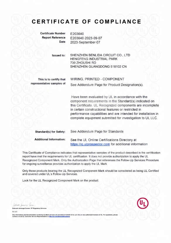
Our Certificates
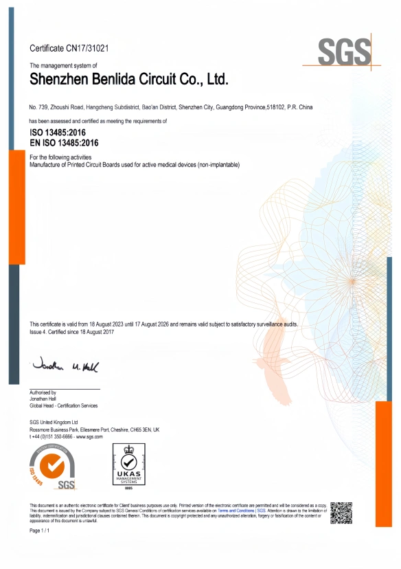
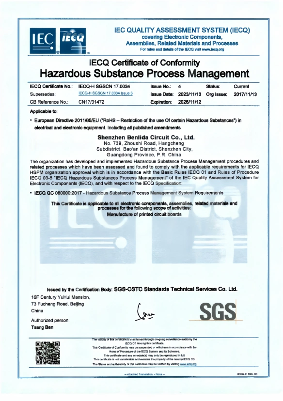
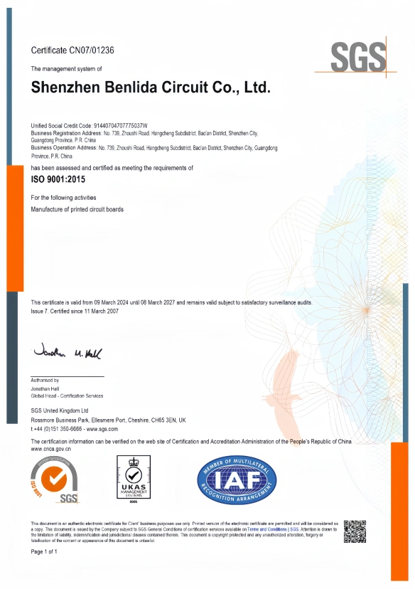
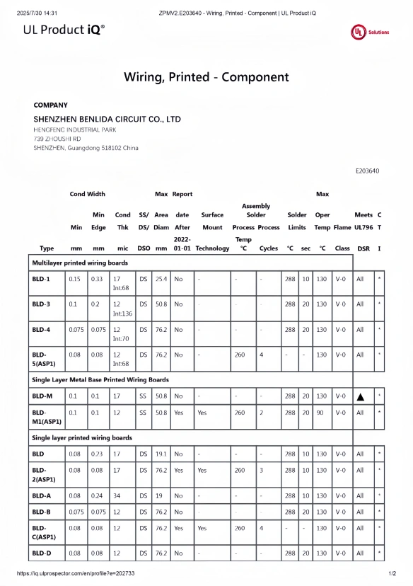
Benlida Circuit is a professional manufacturer of printed circuit boards (PCBs), providing reliable PCB manufacturing services with a strong track record since 2011. We are proud to hold multiple international certifications that demonstrate our commitment to quality, safety, and environmental responsibility, ensuring trusted PCB board service for customers worldwide.

FAQ
Benlida provides various PCB solutions, including FR-4 PCB, multilayer PCB, HDI PCB, high-frequency PCB, heavy copper PCB, rigid-flex PCB, FPC, and LED PCB. We offer suitable PCB solutions based on different application requirements and product designs.
Yes. Benlida supports custom bare-PCB requirements based on customer project files. Options may include PCB type, stack-up, materials, copper weight, surface finish, impedance requirements, tolerances, and bare-board electrical testing, subject to engineering review.
Inspection and testing for bare PCBs may include visual or automated optical inspection of circuitry, dimensional checks, and project-defined electrical testing for continuity and isolation. The method, coverage, acceptance criteria, and required records should be confirmed for the order.
Yes, Benlida supports PCB production from prototype development to mass manufacturing. With flexible production capabilities and professional PCB board service, we help customers move smoothly from design verification to larger-scale production according to their project needs.
For a bare PCB quote, provide the available fabrication data in the format agreed for the quote, together with NC Drill data when it is separate, the fabrication drawing, revision, quantity, board construction, material, finished thickness, copper weight, surface finish, and any impedance, tolerance, or test requirements. Mark any item that is not yet defined for review.