Skip to content
+8613590338876
sales@szbldpcb.com
Home
Capabilities
Solutions
Quality Control
About
Blog
Contact Us
Request a Quote
PCB Manufacturing
FR-4 PCB
Multilayer PCB
HDI PCB
High-Frequency PCB
Heavy Copper PCB
Rigid-Flex PCB
FPC
LED PCB
Ceramic PCB
PCB Assembly
SMT
DIP
Firmware Flashing
Functional Testing
Engineering Services
PCB Layout
PCB Upgrade
Products Development
Reverse Engineering
Engineering Consults
Manufacturing Services
Alternative Components
Wire Harness
3D Printing
Injection Molding Services
CNC Machining Services
Box Build
Consumer Electronics
Industrial Automation
Medical Devices
Automotive Electronics
Telecommunications
Aerospace Electronics
Home
Capabilities
Solutions
Quality Control
About
Blog
Contact Us
Request a Quote →
Blogs
Home
»
Blog
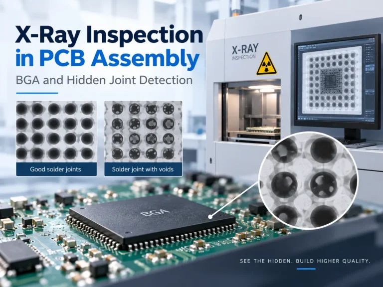
X-Ray Inspection in PCB Assembly — BGA and Hidden Joint Detection
September 12, 2026
Read More >>
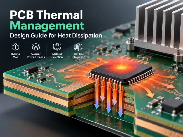
PCB Thermal Management — Design Guide for Heat Dissipation
September 11, 2026
Read More >>
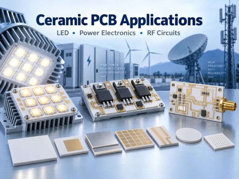
Ceramic PCB Applications — LED, Power Electronics & RF Circuits
September 10, 2026
Read More >>
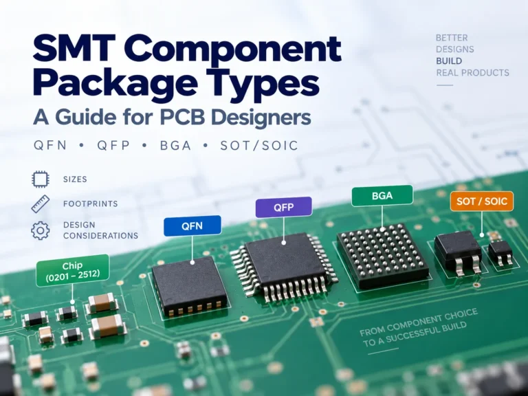
SMT Component Package Types — A Guide for PCB Designers
September 9, 2026
Read More >>
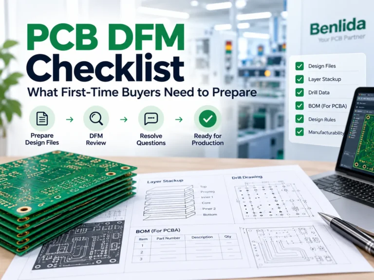
PCB DFM Checklist — What First-Time Buyers Need to Prepare
September 8, 2026
Read More >>
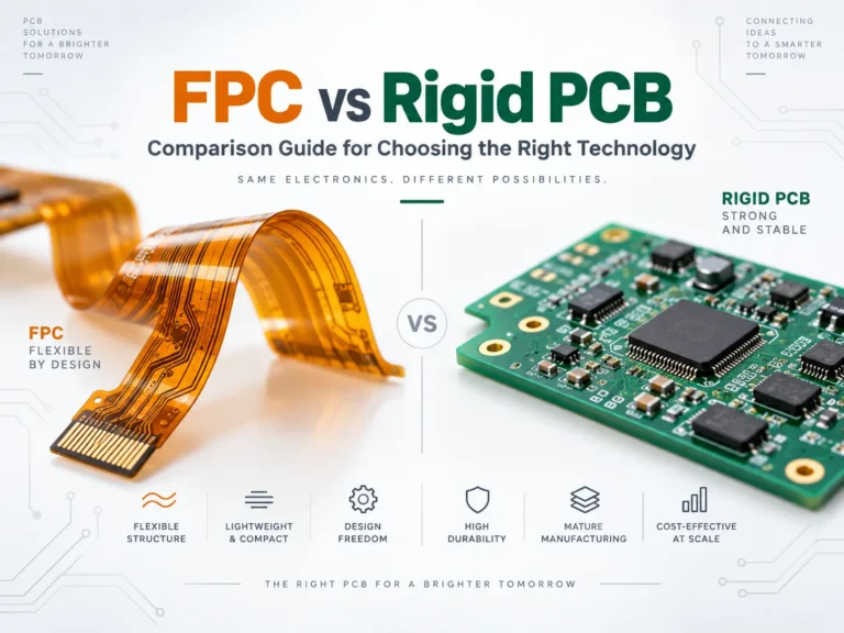
FPC vs Rigid PCB — Comparison Guide for Choosing the Right Technology
September 7, 2026
Read More >>
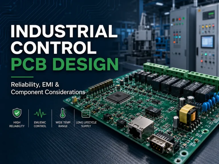
Industrial Control PCB Design — Reliability, EMI & Component Considerations
September 2, 2026
Read More >>
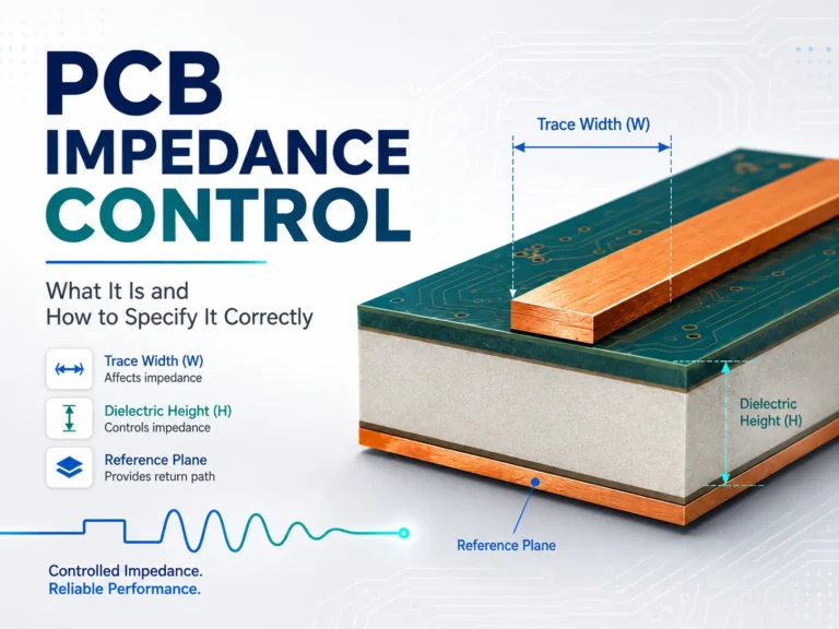
PCB Impedance Control — What It Is and How to Specify It Correctly
September 2, 2026
Read More >>
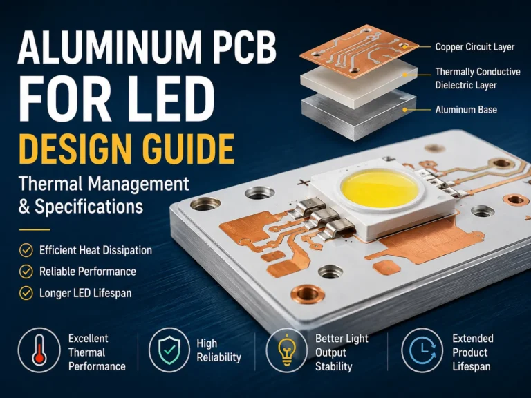
Aluminum PCB for LED — Design Guide, Thermal Management & Specifications
September 1, 2026
Read More >>
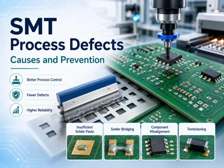
SMT Process Defects — Causes and How to Prevent Them
August 29, 2026
Read More >>
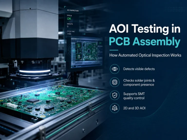
AOI Testing in PCB Assembly — How Automated Optical Inspection Works
August 28, 2026
Read More >>
PCB BOM Preparation Guide: What Your PCBA Supplier Needs
August 27, 2026
Read More >>
No posts found
1
2
3
4
Next
Scroll to Top
Contact Us
Name
Email
Country
Message
upload
Submit
→
Contact Us
Contact Form
WhatsApp
Email