
Support from prototype development to mass production
Telecommunications Electronics PCB Manufacturing & PCB Assembly Services
Benlida provides reliable pcb communication solutions for telecommunications electronics manufacturers, offering integrated PCB fabrication, turnkey PCBA assembly, engineering support, and testing services. With advanced production technology, strict quality control systems, and experienced engineering teams, we help customers develop high-performance circuit boards for communication equipment, network systems, and other advanced electronic devices, supporting projects from prototype development to volume production.
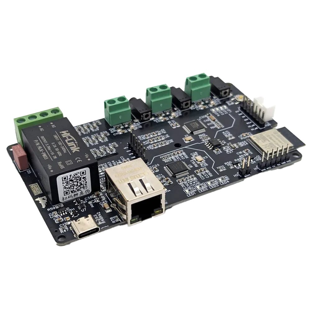
Telecommunications Electronics Manufacturing Capabilities
Benlida provides comprehensive PCB manufacturing capabilities for telecommunications electronics, covering PCB fabrication, PCB assembly, engineering services, and testing solutions. With advanced manufacturing equipment, experienced engineers, and standardized quality management systems, we deliver reliable pcb communication solutions for communication equipment, network systems, and connected electronic products. Our capabilities include multilayer PCB manufacturing, HDI PCB, flexible circuit solutions, SMT assembly, and customized testing services to support different communication applications.
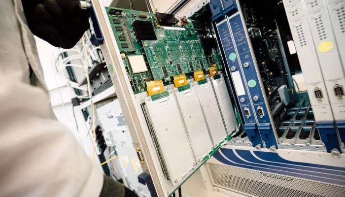
PCB Fabrication
Benlida provides advanced PCB fabrication services for telecommunications electronics, supporting pcb communication projects that require stable signal transmission, reliable electrical performance, and long-term operation.
Our PCB fabrication capabilities include:
• Multilayer PCB Manufacturing
Facilitates complicated circuit layout that allows high density routing and electrical conductivity for modern communication devices.
• HDI PCB
Provides compact, high-density circuit solutions for communication devices requiring optimized layouts and efficient signal transmission.
• Flex PCB & Rigid-Flex PCB
Offers flexible circuit solutions for communication products with compact structures and complex installation requirements.
• Controlled Impedance PCB
Enables proper signal transfer for high speed communication systems.
• Thick Copper PCB
Provides enhanced current carrying capability and thermal performance for communication equipment with higher power requirements.
PCB Assembly
Benlida provides turnkey PCB assembly services for telecommunications electronics, combining advanced assembly technologies and strict quality control to support reliable communication products.
Our PCB assembly capabilities include:
• SMT Assembly
Provides high-precision component placement for communication modules, networking equipment, and electronic devices.
• DIP Assembly
Supports through-hole component assembly for applications requiring strong mechanical connections and durability.
• Mixed PCB Assembly
Combines SMT and DIP technologies to meet complex assembly requirements for communication products.
• BGA Assembly
Supports high-density components used in advanced communication systems and electronic devices.
• Box Build Assembly
Provides complete product integration services, including PCB assembly and final system assembly.
Engineering Services
Benlida provides engineering support to improve PCB manufacturability, optimize designs, and reduce development risks for telecommunications electronics projects.
Our engineering services include:
• DFM Review
Identifies potential manufacturing issues in communication PCB designs before production.
• DFA Optimization
Improves assembly efficiency and manufacturing consistency for electronic products.
• BOM Verification
Helps ensure component availability and stable production throughout the manufacturing process.
• Component Sourcing
Provides sourcing support to improve supply chain reliability and reduce production delays.
• Engineering Consultation
Offers technical guidance from initial design review to mass production.
Testing Services
Testing is very important for the electronics in telecommunications that must run reliably. Benlida applies comprehensive inspection methods to verify the quality and reliability of pcb communication products.
Our testing capabilities include:
• AOI Inspection
This detects errors in soldering, positioning of components, and any other assembly-related issues.
• X-Ray Inspection
Checks hidden solder joints and complex component connections such as BGA assemblies.
• ICT Testing
Verifies electrical performance and identifies circuit defects in PCB assemblies.
• Functional Testing
Confirms product operation under actual working conditions.
• Customized Testing Solutions
Provides testing methods based on specific communication product requirements and application needs.
Communication PCB Applications
The rapid development of 5G networks, IoT technology, and intelligent communication systems has increased demand for reliable circuit solutions. Benlida provides pcb communication solutions designed for applications requiring stable signal transmission, high reliability, and consistent manufacturing quality.
Network Communication Equipment
PCB solutions are widely used in routers, switches, gateways, and network infrastructure equipment that require continuous operation and reliable data transmission.
Wireless Communication Devices
Communication circuit boards support wireless modules, connectivity devices, and electronic products requiring high-frequency performance and controlled impedance design.
IoT Communication Systems
Benlida provides PCB manufacturing support for IoT terminals, smart devices, and connected systems requiring compact designs and stable communication performance.
Data Transmission Equipment
High-density PCB technologies support servers, communication modules, and data processing equipment requiring reliable signal integrity.
Industrial Communication Systems
PCB solutions are used in industrial networking equipment, control systems, and communication devices operating in demanding environments.
Key Challenges in Telecommunications Electronics Manufacturing
Telecommunications electronics demand dependable circuit solutions that deliver excellent signal performance, space efficiency, consistent operation, and lasting reliability.As communication technologies continue to evolve, manufacturers need experienced partners that can support advanced designs, efficient production processes, and consistent product quality for pcb communication applications.
Benlida helps customers overcome these challenges through integrated PCB fabrication, assembly, engineering support, and testing capabilities.
High-Speed Signal Performance
Communication products require stable data transmission and precise signal control, especially in high-frequency and high-speed applications. Benlida supports advanced PCB technologies, including controlled impedance PCB and high-density circuit designs, to help maintain signal integrity and reliable electrical performance.
Complex PCB Design Requirements
Modern communication devices require smaller form factors, higher integration levels, and increasingly complex circuit structures. Benlida supports multilayer PCB, HDI PCB, and flexible PCB technologies to help customers develop compact and reliable electronic products.
Rapid Technology Updates
Wireless networks, IoT platforms, and connected devices are constantly advancing, driving the need for higher standards and improved performance capabilities. Benlida provides rapid prototyping, engineering optimization, and flexible production capabilities to help customers efficiently adapt to updated designs.
Component Supply Stability
Communication products often involve complex components and long production cycles, requiring effective supply chain management. Through BOM verification, component sourcing support, and production planning, Benlida helps customers improve material availability and maintain stable manufacturing schedules.
Product Reliability and Testing
Communication equipment requires continuous operation and consistent performance in different environments. Benlida applies strict quality control processes and comprehensive testing methods, including AOI, X-ray inspection, ICT, and functional testing, to ensure reliable PCB and PCBA performance.
Faster Production and Delivery
Shorter product cycles require efficient transitions from prototype development to mass production. With integrated PCB fabrication, assembly, engineering, and testing services, Benlida provides efficient pcb communication solutions to help customers shorten production timelines and accelerate product launches.
Turn Your Dreams Into Reality
Getting a custom PCB made is simple with Benlida. Submit your design files or project details, and our team will provide a fast, accurate quote tailored to your requirements. Whether it’s a prototype or large-scale production, we make the process easy and efficient.
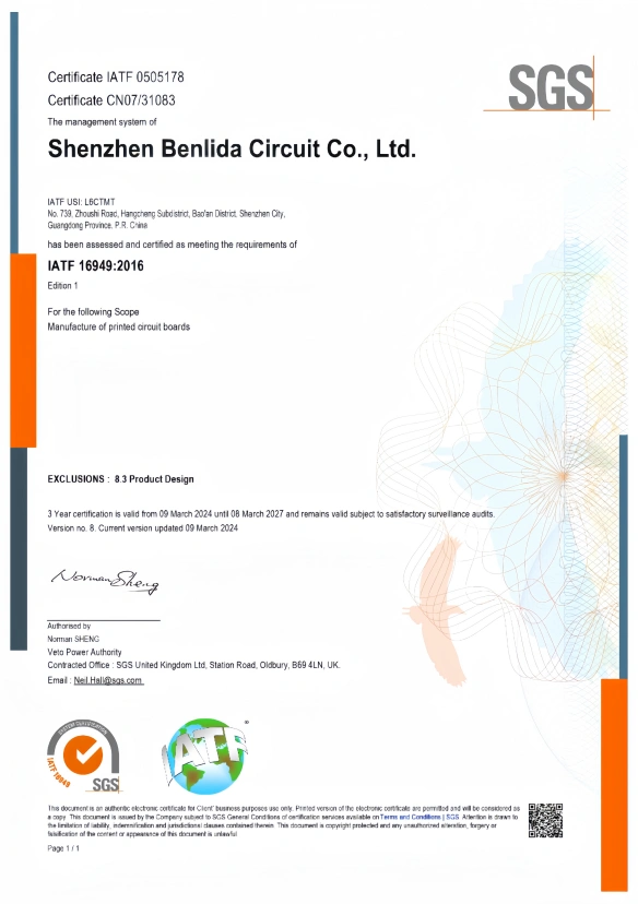
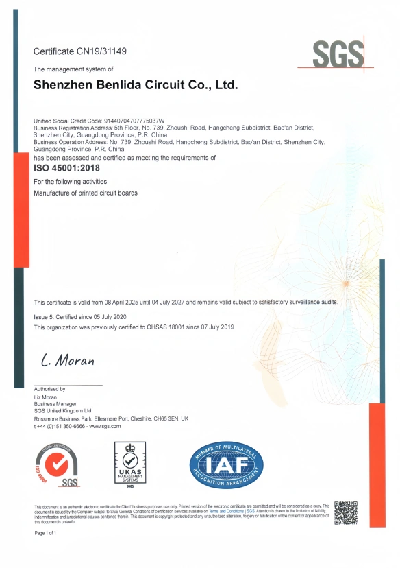
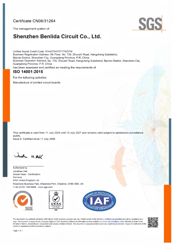
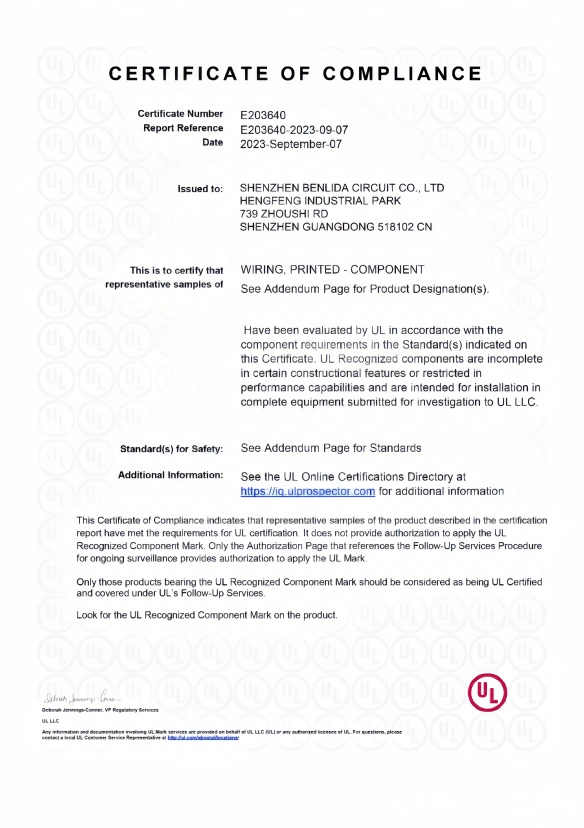
Our Certificates
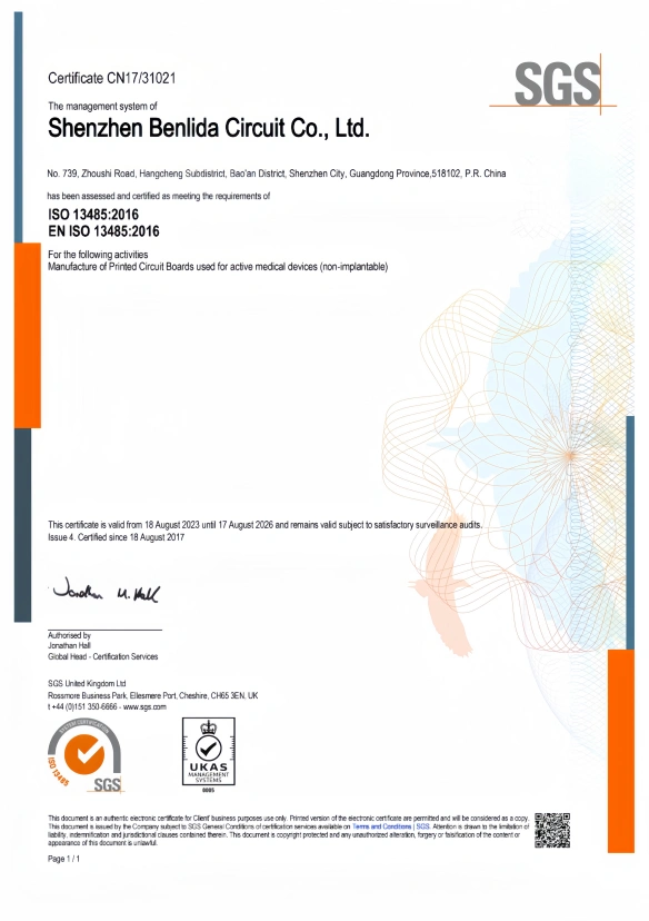
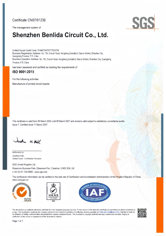
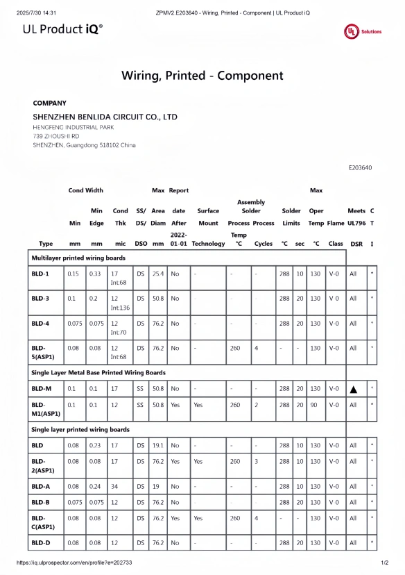
BenlidaPCBA follows internationally recognized quality, environmental, and compliance standards to ensure reliable PCB manufacturing and assembly performance.
Our certifications include:
• ISO 9001 Quality Management System
Ensures standardized manufacturing processes and consistent quality control throughout PCB fabrication and assembly.
• ISO 14001 Environmental Management System
Demonstrates responsible environmental management and sustainable PCB manufacturing practices.
• RoHS Compliance
Ensures PCB products meet international restrictions on hazardous substances and material safety requirements.
• REACH Compliance
Supports responsible chemical management and compliance with global material control standards.
• IPC Standards Compliance
Supports reliable PCB manufacturing and assembly quality through recognized industry guidelines.


Why Choose Benlida for PCB Communication Manufacturing?
Benlida provides reliable PCB manufacturing solutions for telecommunications electronics by integrating PCB fabrication, PCBA assembly, engineering support, and testing capabilities. With experienced manufacturing teams, advanced production equipment, and strict quality control systems, we help customers develop reliable circuit solutions for communication equipment and electronic systems.
Experience in PCB Manufacturing
With years of experience in PCB manufacturing and PCBA assembly, Benlida supports various electronic industries with reliable production capabilities.
Our team understands the requirements of communication-related products, including high-density designs, signal integrity, controlled impedance, and stable electrical performance from prototype development to mass production.
Complete Manufacturing Capabilities
Benlida provides integrated services covering PCB fabrication, SMT assembly, DIP assembly, testing, and box build assembly.
This complete manufacturing process enables efficient pcb communication solutions while helping customers simplify supplier management and improve production efficiency.
Advanced PCB Technology
Benlida supports advanced PCB technologies, including multilayer PCB, HDI PCB, flex PCB, rigid-flex PCB, and controlled impedance PCB.
These capabilities help meet the requirements of communication products that require compact designs, reliable signal transmission, and consistent performance.
Strict Quality Control
Quality and reliability are essential for electronic products that require stable operation.
Benlida applies comprehensive quality control processes, including AOI inspection, X-ray inspection, ICT testing, and functional testing, to ensure consistent manufacturing quality.
Fast Turnaround and Engineering Support
Benlida provides flexible production schedules, rapid prototype support, and professional engineering services throughout the product development process.
Through DFM review, DFA optimization, BOM verification, and technical consultation, we help customers improve product manufacturability and reduce development risks.
FAQ
PCB communication refers to printed circuit board solutions designed for communication-related electronic systems, supporting signal transmission, data processing, and connectivity applications.
Communication electronics commonly use multilayer PCB, HDI PCB, flex PCB, rigid-flex PCB, thick copper PCB, and controlled impedance PCB designs.
Yes. Benlida offers complete PCB assembly services, including SMT assembly, DIP assembly, mixed assembly, BGA assembly, testing, and box build integration.
Benlida applies advanced inspection technologies, including AOI, X-ray inspection, ICT, and functional testing, combined with strict quality management systems.
Yes. Benlida supports projects from prototype development to large-scale production with flexible PCB fabrication and assembly capabilities.
Communication PCB solutions are commonly used in network equipment, wireless devices, IoT systems, industrial communication products, and data transmission equipment.