The widespread commercialization of PCIe 4.0 and PCIe 5.0 server products has increased the demand for high-speed PCBs.
As technologies such as PCIe 6.0 continue to develop, controlling PCB insertion loss has become a critical measure in the high-speed PCB manufacturing process.
The factors influencing signal loss primarily include design, materials, conductor resistance, dielectric thickness, conductor roughness, conductor thickness, and trace width. Design and substrate materials cause the dominant losses, followed by the influence of manufacturing processes; Figure 1 shows the specific proportions of these influences. This paper focuses on researching the impact of high-speed PCB manufacturing processes on signal loss.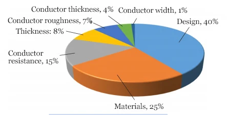
Test Section
For this study, the experiment used reverse-treated copper foil (RTF) with varying surface roughness.The experiment tested three different browning solutions.
It also tested various circuit surface roughening methods and solder mask inks with different dielectric loss (Df) values.
The experiment included both back-drilled and non-back-drilled conditions as factors influencing signal loss.
-
Test Layouts and Stackup Design
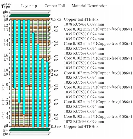
Using the Delta-L 4.0 standard test module (as shown in Figure 2), the experiment designed 5-inch (127 mm) and 10-inch (254 mm) dual-line structures.
These structures meet the loss testing requirements for high-frequency signals (1–40 GHz).
The module includes calibration and test sections, which eliminate additional loss and interference from fixtures and connection points.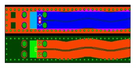
-
Test Materials and Equipment
-
Test Protocol
This protocol uses Delta-L 4.0 as the module testing method.
It employs the controlled variable method to investigate the effect of different RTF copper foils on insertion loss.
The study examines various combinations of browning treatments, outer layer pretreatments, and solder mask pretreatments.
It also tests different solder mask ink types, back-drilling processes, and numbers of reflow cycles.
After the finished test boards pass continuity testing, a vector network analyzer measures insertion loss. Each test condition repeats three times, and the process calculates the average as the final result to ensure data reliability.Test Plan Design and Evaluation Factors
Table 1 presents the test plan, and Table 2 lists the specific parameter values for each factor.| Variable Type | Test Item | Number of Factors | Specific Factors |
|---|---|---|---|
| Material Variables | RTF Copper Foil | 5 | RTF1, RTF2, RTF3, RTF4, RTF5 |
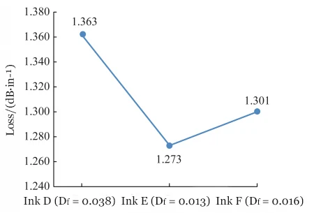
| Material Variables | Solder Mask Ink | 3 | Standard D Ink A, Low D Ink E, Low D Ink F |
| Material Variables | Brown Oxide Treatment | 3 | Brown Oxide A, Brown Oxide B, Brown Oxide C |
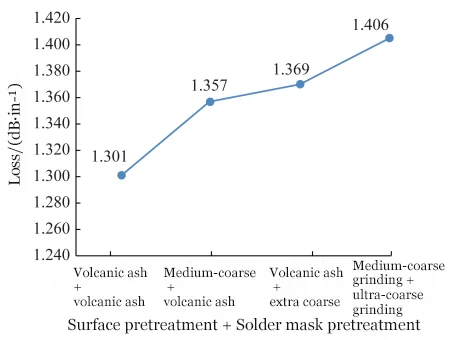
| Process Variables | Outer Layer Pre-treatment & Solder Mask Pre-treatment Combination | 4 | Volcanic Ash + Volcanic Ash; Medium Roughening + Volcanic Ash; Volcanic Ash + Ultra Roughening; Medium Roughening + Ultra Roughening |
| Process Variables | Back Drilling | 2 | With Back Drilling; Without Back Drilling |
| Process Variables | Reflow Soldering | 3 | 1 Reflow Cycle; 3 Reflow Cycles; 5 Reflow Cycles |
Tab 1: Insertion Loss Test Plan Design
Material Properties and Process Parameters
| Item | Type | Key Parameters | Remarks |
|---|---|---|---|
| Substrate | Ultra-low loss substrate | Dk / Df (10 GHz): 3.25 / 0.0040 | / |
| Copper Foil | RTF1 ~ RTF5 | RTF1–RTF5 Rz values respectively: 6.36, 5.53, 4.69, 2.36, 0.60 μm | Supplier provides copper foil roughness as Rz (linear data); this paper mainly uses surface data Sz to represent roughness |
| Solder Mask Ink | Standard Df ink D; Low Df solder mask ink E/F | Ink D: Dk / Df (10 GHz): 3.25 / 0.0040Ink E: Dk / Df (10 GHz): 3.15 / 0.0013Ink F: Dk / Df (10 GHz): 3.17 / 0.0016 | — |
| Key Parameter: Micro-etch Amount | Inner layer pre-treatment; Brown oxide A, B, C; Volcanic ash; Medium roughening; Ultra roughening | Inner layer pre-treatment: 0.40–1.20 μmBrown oxide A: 0.18–0.27 μmBrown oxide B/C: 1.00–1.60 μmVolcanic ash: no micro-etchMedium roughening: 0.60–1.40 μmUltra roughening: 0.80–1.40 μm | Inner layer: inner layer pre-treatment, brown oxide A/B/COuter layer: volcanic ash, medium roughening, ultra roughening |
| Back Drilling | Back drill stub | Back drill stub control: 0–12 mil | — |
| Reflow Soldering | Lead-free reflow soldering | Lead-free reflow conditions: (260±5)°C for 20 s; >217°C for 120–150 s | — |
Tab 2: Specific Parameter Values Corresponding to Each Factor
-
Process Flow
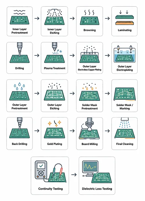
Results and Discussion
-
Effect of Browning Treatment on Signal Loss for Different RTF Copper Foils
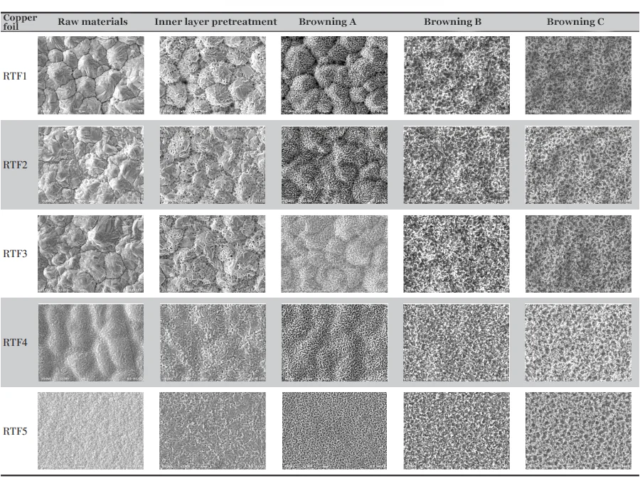
1. Morphological Changes After Browning
The browning process has a significant effect on the morphology of copper foil. After Browning A treatment, only a shallow honeycomb-like structure appeared on the surface of the copper foil, with minimal morphological changes;Browning B and Browning C treatments created distinct honeycomb-like pitting on the copper foil surface.
Browning C produced the greatest pitting depth and the most pronounced honeycomb structure.
These results align with the micro-etching control range of the browning solution (Browning A < Browning B = Browning C).
2. Overall Roughness of Copper Foil
The corrosiveness of the browning solution primarily affects the degree of surface undulation of the copper foil.
The initial state of the raw copper foil determines the height of the surface peaks and valleys.
Together, these two factors determine the overall roughness characteristics of the copper foil.
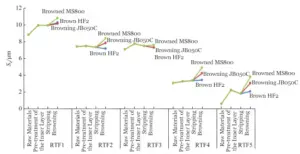
The changes in Sdr after treatment of different RTF copper foils are shown in Figure 4, and the changes in Sz are shown in Figure 5. The specific patterns are as follows:(1) Sdr Variation Pattern
Browning A results in the smallest increase in Sdr (average increase <5%), while Browning B and Browning C result in larger increases in Sdr (average increase >15%), with Browning C showing a slightly higher increase than Browning B.(2) Patterns of Sz variation
The effect of browning on Sz is relatively small (change rate <10%). RTF1 has the largest Sz (raw material Sz ≈ 6.5 μm), while RTF5 has the smallest Sz (raw material Sz ≈ 0.6 μm). After undergoing the same process treatment, the relative order of Sz for each copper foil remains unchanged.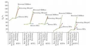
3. Insertion Loss Test Results
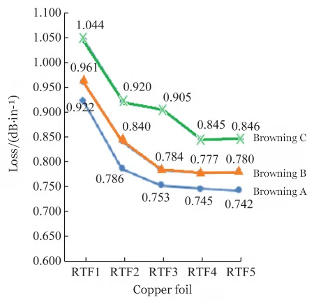
Figure 6 shows the variation in signal insertion loss for different RTF copper foils under different browning treatments. Under the same browning process, signal loss decreases as copper foil roughness decreases, fully matching the trends for Sdr and Sz, showing that copper foil roughness strongly affects signal loss. For the same type of copper foil: signal loss increases as the corrosiveness of the browning solution increases, specifically manifested as Browning C > Browning B > Browning A. Stronger corrosiveness of the browning solution increases the Sdr on the copper foil surface. This increase amplifies signal attenuation caused by the skin effect.In high-speed PCB manufacturing, selecting low-roughness RTF copper foil, such as RTF4 or RTF5, reduces signal loss in inner-layer circuits.
Pairing it with a low-corrosivity browning solution, such as Browning A, further improves signal integrity.
-
The Effect of Outer Layer Pretreatment and Solder Mask Pretreatment Combinations on Signal Loss
-
The Effect of Top-Layer Solder Mask Ink on Signal Loss
-
The Effect of Back Drilling on Signal Loss in Signal Vias
(1) Low-frequency Band (4 GHz)
The difference in signal loss between back-drilled and non-back-drilled holes is small, and the parasitic effects of the stub are not significant.(2) High-frequency Band (8 GHz and above)
Signal loss without back-drilling is significantly higher than with back-drilling, and the difference increases with higher frequencies. At 16 GHz, signal loss without back-drilling is 0.102 dB/in higher than with back-drilling, representing a difference of 13.5%. Analysis shows that as frequency increases, the parasitic reactance of the stump increases, leading to more severe signal reflection and attenuation within the stump. Therefore, for high-speed PCBs operating at frequencies of 8 GHz or higher, the back-drilling process for signal vias is a necessary measure to suppress high-frequency signal loss, effectively improving signal transmission integrity and reliability.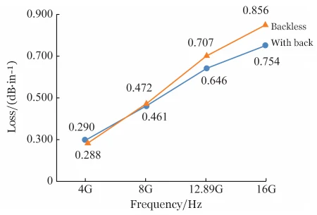
-
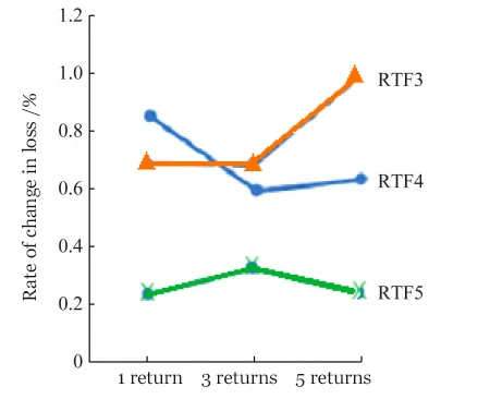
The Effect of Reflow Soldering on Signal Loss