

High-Performance HDI PCB Supplier
HDI PCB
Benlida is a reliable HDI PCB supplier specializing in advanced HDI PCB manufacturing. We provide high-density interconnect boards with precise circuit structures and reliable performance for compact and high-performance electronic applications.
Proposed build-up and microvia structure
Material, thickness, and impedance requirements
Current revision, quantity, and production stage
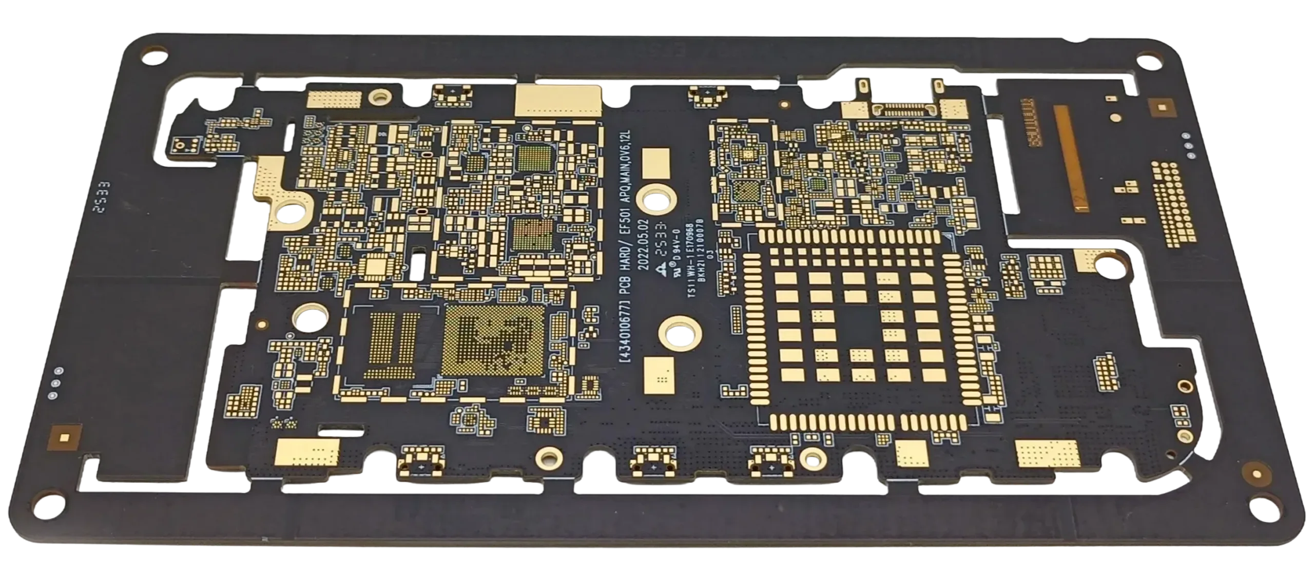
What is an HDI PCB?
A High-Density Interconnect Printed Circuit Board is a type of printed circuit board specially engineered for miniaturized and high-speed electronic products. As an advanced printed circuit board solution provided by an HDI PCB supplier and manufacturer, the HDI PCB uses fine traces, small vias, and multilayer construction to achieve high efficiency and minimize the size of the board.
When compared to regular printed circuit boards, HDI boards provide improved wiring density and increased signal performance by utilizing technologies such as microvias, fine lines, and multilayers.
Related PCB services: Use this page for rigid HDI build-up and microvia fabrication. For conventional multilayer boards without an HDI build-up, see multilayer PCB manufacturing. For the broader bare-board scope, see PCB manufacturing services. If one board combines rigid and flexible sections, see rigid-flex PCB manufacturing.
Materials and signal requirements: For laminate-family terminology and grade selection, see FR-4 PCB materials. When Dk, Df, insertion-loss, or RF and microwave requirements drive stack-up decisions, see high-frequency PCB manufacturing.
Assembly, design, and quotation: If the project also requires component sourcing, SMT/THT assembly, or assembled-board testing, see PCB assembly services. For stack-up, microvia arrangement, trace spacing, and DFM file preparation, use our HDI PCB design rules and DFM file checklist. When the current project data is ready, use the HDI PCB RFQ checklist before requesting a quote.
Microvias
Provide complex interconnection capability within the PCB layers, thereby enabling more components to be incorporated within smaller designs.
Fine Lines & Spacing
Support advanced component layouts and high-density routing requirements for modern electronic applications.
Reduced Size & Weight
Make HDI PCBs ideal for portable devices, wearable electronics, and other space-constrained products.
Enhanced Performance
Shorter signal paths improve transmission speed, electrical performance, and signal integrity.
Our HDI PCB Manufacturing Capabilities
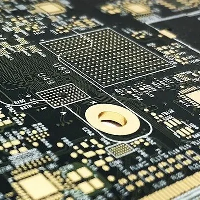
Benlida provides reliable HDI PCB manufacturing solutions with advanced capabilities in microvia, blind/buried via, laser drilling, and fine-line technologies. As an experienced HDI PCB supplier and manufacturer, Benlida delivers high-quality HDI boards with precision, reliability, and flexibility to support modern electronic applications requiring high-density and miniaturized designs.
MOQ
1 pcs
High Layer Count Support
4-32 layers
Via Diameter
50-150 μm (2-6 mils)
OEM/ODM
available
BGA Pitch Supported
Down to 0.25mm
Advanced Surface Finishes
ENIG, Immersion Silver, lead-free options
Drilling Method
Laser drilling+mechanical
Manufacturing Cost
Higher (1.5x to 4x)
Via Structure Details
Layer spans, blind/buried connections, stacked or staggered arrangements, and fill/cap requirements
Aspect Ratio
0.75:1 to 1:1 for microvias
Precision Assembly Support
Fine-pitch, BGA, CSP, QFN for high-density assembly
Testing & Quality Assurance
AOI, X-ray, flying probe, ICT; IPC & ISO 9001 compliant
Material Expertise
FR-4, Rogers, specialty substrates, flexible & rigid-flex
Fine Line & Space Capability
Minimum trace/space: 3/3 mil (0.075/0.075 mm)
Packaging
ESD Protection Materials, Moisture barrier bags, Bubble wrap, Corrugated cartons
HDI Build-Up Structures and Microvia Arrangements
In common HDI notation, 1+N+1 and 2+N+2 describe the build-up layers added to each side of a central multilayer substructure. N denotes the number of conductive layers in that substructure. The complete stack-up and fabrication documentation define the via spans, drilling method, fill or cap construction, materials, and product requirements.
The descriptions below explain common HDI structure terminology. Project availability depends on the submitted stack-up and fabrication requirements.
Build-Up Notation
1+N+1
One build-up layer is added to each side of a central multilayer substructure. The stack-up must specify via spans, dielectric construction, pad geometry, fill or cap requirements, and impedance requirements.
2+N+2
Two build-up layers are added to each side. The stack-up must state the sequential build-up route and whether adjacent microvias are stacked or staggered. It must also specify via-fill, planarity, dielectric, and product requirements.
Higher-Order Build-Up
Higher-order build-up uses three or more build-up layers on one or both sides of the central substructure. Additional build-up steps and interfaces increase the number of manufacturing considerations. Manufacturability depends on the complete construction and project requirements.
Microvia Arrangement
Staggered Microvias
Staggered microvias are offset from one another in successive build-up layers. Selection factors include the offset, via spans, pad geometry, dielectric construction, routing space, and product requirements.
Stacked Microvias
Stacked microvias are vertically aligned through successive build-up layers. Selection factors include stack height, via-fill and cap construction, interfacial connections, materials, assembly conditions, and product requirements.
Via Placement and Span
Via-in-Pad
Via-in-pad places a via within a component land. The fabrication documentation must specify the via type and indicate which of the following conditions apply: open, filled, capped, and planarized. It must also specify acceptance requirements for voids or dimples, surface finish, and assembly. A filled and plated-over implementation should be specified explicitly as via-in-pad plated over (VIPPO).
Skip Microvia
A skip microvia connects nonadjacent conductive layers while bypassing one or more intermediate layers without connecting to them. Its manufacturability depends on via depth, dielectric construction, target-land geometry, and the complete stack-up.
Interconnection Architecture
Any-Layer / ELIC
Any-layer HDI, often described as every-layer interconnection (ELIC), typically uses filled microvia interconnections through successive layers. The fabrication documentation must specify the permitted layer pairs and selected build-up construction. It must also specify the stacked or staggered arrangement, fill or cap construction, materials, build-up route, and product requirements.
Advantages of HDI PCBs
Higher Circuit Density
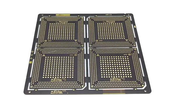
HDI circuit boards employ innovative technologies, including microvias, blind vias, and buried vias that can help attain high-density wiring on the circuit board despite the small board size.
Smaller Size and Reduced Weight
The HDI board can help a lot in making sure that the size and weight of the board are reduced using the appropriate strategy during the process of interconnecting and not using traditional through-holes.These kinds of circuit boards are suitable for applications requiring small electronics, including portable devices.
Improved Signal Integrity
The shortened signal lines and the routing design on the HDI boards can improve the transmission loss and minimize the interference problems.
Support for High-Density Component Assembly
HDI technology supports fine-pitch components such as BGA, CSP, and QFN, enabling more efficient component placement and higher integration levels for advanced electronic designs.
Flexible Design Options
With different structures, including single-sided microvia HDI, double-sided microvia HDI, stacked microvia HDI, and sequential laminated HDI, a professional HDI PCB supplier like Benlida can provide suitable solutions based on different product requirements.
Wide Range of Applications
With advantages in size, performance, and reliability, HDI PCBs are widely used in consumer electronics, medical equipment, automotive electronics, communication devices, and industrial control systems.
Why Choose Benlida as Your HDI PCB Supplier
Benlida specializes in HDI board manufacturing and supply. This company implements the latest technologies in the manufacturing process, as well as performs strict control over it. Using years of experience with HDI technologies, Benlida makes its customers able to design HDI PCBs.
Advanced HDI Manufacturing Capability
Benlida has strong HDI manufacturing capabilities, supporting advanced technologies such as microvias, blind vias, buried vias, stacked microvias, and any-layer interconnections. This will ensure that complex circuits can be designed with ease.
Stable and Reliable Product Quality
Quality is one of the major concerns of the entire production process. Benlida follows stringent quality control practices and advanced inspection techniques, such as AOI, X-ray inspection, flying probe testing, and ICT. In this way, it ensures that all its products have stable electrical properties and high reliability.
Flexible Customization and Production Support
By having various designs, such as single-sided microvia HDI, double-sided microvia HDI, stacked microvia HDI, and sequential laminated HDI, it is possible to get proper answers from a professional HDI PCB manufacturer like Benlida according to various product needs.
Support for High-Density Component Assembly
Benlida’s HDI manufacturing capabilities support fine-pitch components such as BGA, CSP, and QFN, helping customers achieve higher integration levels and more compact electronic product designs. These HDI boards are suitable for applications that require efficient space utilization and reliable performance.
Efficient Delivery and Professional Service
With well-established production management processes, standardized packaging, and professional technical support, Benlida provides dependable delivery and responsive service to customers worldwide.
HDI PCB Manufacturing Process
The eight stages below summarize an HDI fabrication route. The actual route depends on the buried-via substructure, the number of build-up cycles, the microvia arrangement, the materials, the metallization and fill requirements, and the project acceptance plan. In this overview, Steps 3–6 form the lamination–microvia–metallization–circuit cycle and repeat only when the approved stack-up requires another build-up level.
1
HDI Design Review & Process Planning
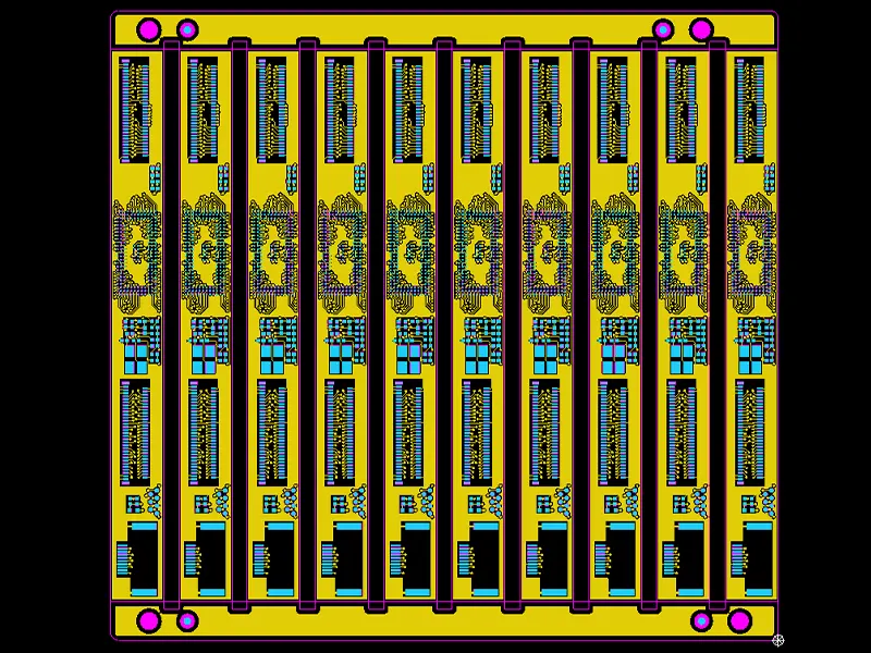
Before fabrication, the PCB data, fabrication drawing, drill files, proposed stack-up, material, impedance, and acceptance requirements are reviewed together. The manufacturing route is defined against the project revision approved for production.
2
Inner-Layer Circuits and Buried-Via Substructure
Inner-layer circuits and any buried-via substructure are fabricated and inspected according to the approved route. The buried-via substructure is drilled using the specified method. After drilling, the applicable sequence of cleaning or desmear, conditioning, metallization, plating, and any required filling, capping, or planarization is completed before subsequent lamination.
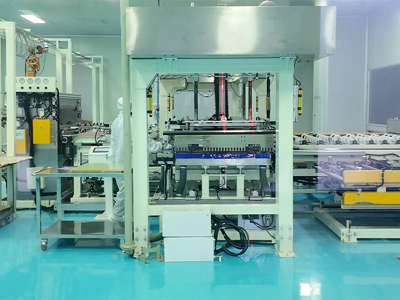
3
Sequential Build-Up Lamination
The specified build-up dielectric and copper are laminated to the prepared substructure according to the approved stack-up. Steps 3–6 repeat only when another build-up level is required.
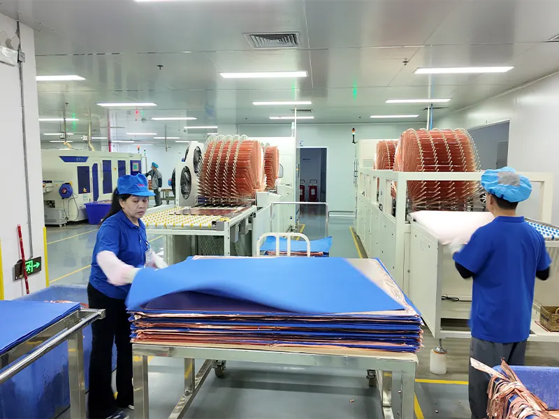
4
Blind-Via and Laser-Microvia Formation
Microvias across the defined dielectric spans are formed using the approved drilling route. Blind and buried describe layer connectivity, while the drilling method is specified separately. Applicable post-drill cleaning, residue removal or desmear, and surface conditioning precede metallization.
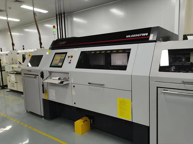
5
Via Metallization, Filling and Planarization
The selected metallization route establishes the initial conductive layer. Where electroless copper is used, electroless copper deposition precedes copper electroplating. For stacked microvias or VIPPO, the fabrication documentation must define filling, cap construction, planarity, interface construction, finished-pad requirements, and agreed void or dimple criteria.
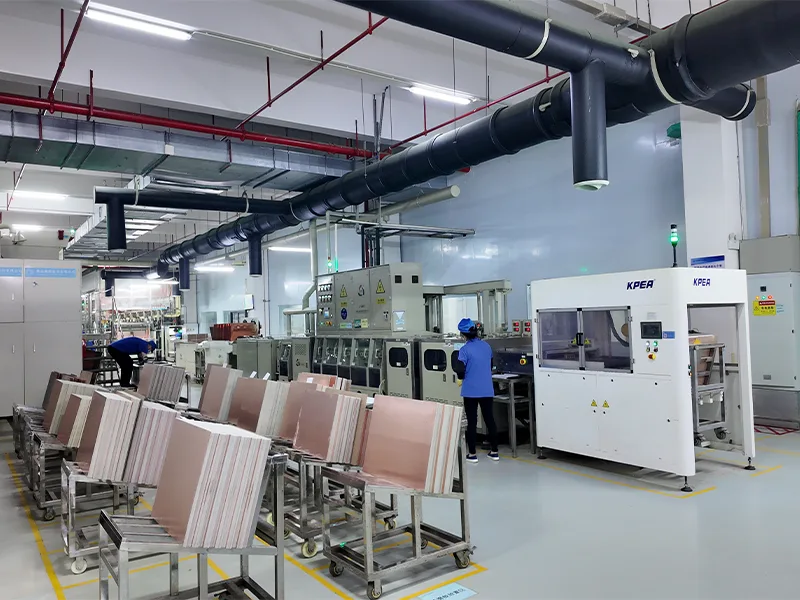
6
Fine Line Circuit Formation
The build-up circuit layer is imaged and formed using the approved patterning route, then inspected at the defined stage. AOI may be used to compare the circuit pattern with released data. If another build-up level is required, the route returns to Step 3.
7
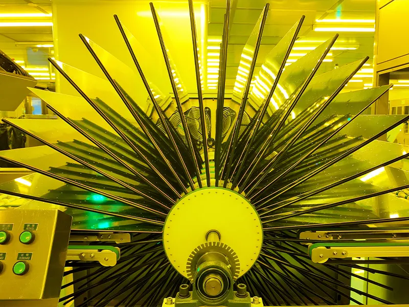
Surface Finishing & PCB Finalization
After the required build-up cycles, final mechanical drilling and plated-through-hole (PTH) processing are completed where specified. Final outer-layer circuit formation and inspection, solder mask, legend, surface finish, and profiling then follow in the order defined for the project.
8
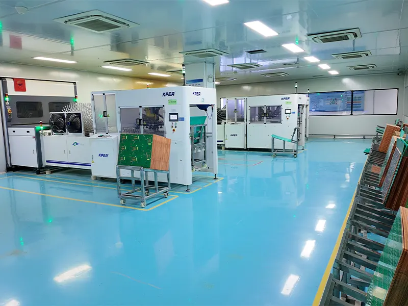
Electrical Testing & Quality Inspection
Final inspection and testing follow the order-specific plan. The plan defines the item or coupon, method, stage, coverage or sampling, acceptance criteria, and record availability.
Define Microvia Reliability Requirements Before Production
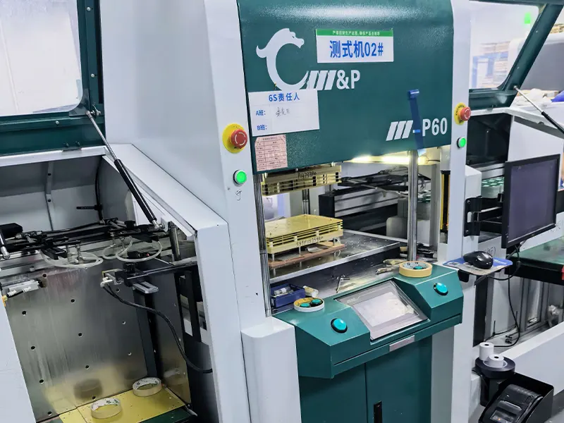
Microvia reliability depends on the complete stack-up, target-pad interfaces, plating and fill construction, materials, fabrication process, and assembly thermal profile. Stacked and staggered arrangements create different interface and routing geometries. The selected structure should therefore be reviewed against the project’s layer transitions, pad geometry, dielectric construction, acceptance criteria, and intended use conditions.
Some microvia interface defects can remain latent at room temperature and appear during reflow or other thermal stress. Each result should identify the inspected or tested item, method, sampling plan, and acceptance criteria. Where thermal stressing with resistance monitoring is specified, also define the representative coupon or sample, thermal profile, cycle count, and resistance-change limit.
Microsection, X-ray, room-temperature electrical testing, convection reflow testing with continuous resistance monitoring, and interconnect stress testing (IST) provide different types of evidence. No single result should be used alone to claim long-term field reliability.
| Method or record | What it can support | What the project must define |
|---|---|---|
| Process traveler / traceability records | Linkage among the delivered lot, material, revision, and recorded process history; supports attribution, not physical reliability evidence | Required identifiers, record scope, linkage to the delivered lot, and record or report availability |
| Microsection | Visible cross-sectional geometry, plating, fill, and interfaces at the examined plane of the sampled section; not lot-wide thermal performance | Structure or coupon, sampling quantity and locations, preparation and evaluation method, acceptance criteria, and report requirements |
| X-ray / CT where specified | Resolvable internal geometry and gross fill, void, or alignment conditions within the selected inspection setup; not interface bond strength or field reliability | Inspection target, method, resolution or voxel size where applicable, views or coverage, sampling, acceptance criteria, and report requirements |
| Netlist electrical test | Network continuity and isolation at the specified test stage and limits; not latent thermomechanical interface performance | Test data source, continuity and isolation limits, coverage, test stage, handling of retest, acceptance criteria, and report requirements |
| Convection reflow with monitored coupon | Resistance behavior of a representative via-chain coupon during specified convection reflow cycles; not direct field-life equivalence | Coupon design and represented structures, conditioning, reflow profile, cycle count, measurement interval, resistance-change limit, sample quantity, acceptance criteria, and report requirements |
| IST or agreed equivalent | Resistance-change and cycles-to-threshold behavior of a representative coupon under the specified accelerated thermal-stress protocol; not direct field-life equivalence | Coupon design and represented structures, conditioning, temperatures, cycle definition, monitoring method, failure threshold, sample quantity, acceptance criteria, and report requirements |
Include only methods or records agreed for the project. The quotation or procurement documentation should define applicability, sampling, acceptance criteria, and report requirements.
HDI PCB Surface Finish
Benlida offers a variety of HDI PCB surface finish options, including HASL, Lead-Free HASL, ENIG, Immersion Tin, Immersion Silver, and OSP to meet different requirements for solderability, surface flatness, and long-term reliability. As an experienced hdi pcb supplier, Benlida provides suitable finishing solutions for different applications, helping improve the performance and manufacturing stability of HDI boards.
HASL
A traditional, cost-effective finish using molten solder, ideal for general-purpose PCBs.
Lead-Free HASL
Environmentally friendly version of HASL, meeting RoHS standards for lead-free electronics.
ENIG
Provides a flat, gold-coated surface for excellent solderability and reliable high-frequency performance.
Immersion Tin
Offers uniform, smooth surface with good solderability for short to medium-term applications.
Immersion Silver
Provides high conductivity and excellent surface planarity for precision assembly and fine-pitch parts.
OSP
Organic solderability preservative protects copper while remaining flat, perfect for fine-pitch components.
HDI PCB Design Guides
Designing of HDI PCB involves taking into account the layer structure, via technology, traces layout, and signal integrity in order to ensure reliable work and proper manufacturing process. Being an experienced HDI PCB supplier, Benlida offers clients professional assistance in designing their products and helps to optimize their HDI structure as well as improve the efficiency of production and minimize possible manufacturing risks.
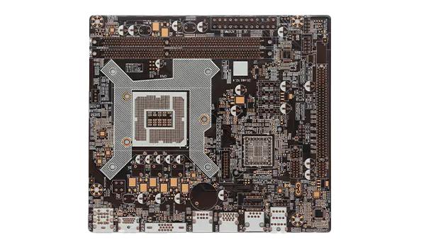
Designing HDI PCBs requires careful consideration of layer structure, via technology, and signal integrity. Following best practices ensures manufacturability, reliability, and optimal performance.
Symmetric Stackup
Plan the number of signal, power, and ground layers carefully to optimize routing density. Using a balanced and symmetric stack-up helps minimize board warpage and improve signal integrity, especially for complex HDI boards with higher layer counts. Sequential lamination is recommended for advanced multilayer designs.
Via Selection
The selection of proper via structure is critical for the creation of reliable high-density interconnections. An experienced HDI PCB supplier will be able to provide clients with appropriate via structures, such as blind, buried, or stacked micro-vias.
Design for Manufacturability (DFM)
It is very important to stick to the DFM rules to have production without problems and maintain high-quality standards. Cooperation with a professional HDI PCB producer makes it possible for designers to adhere to the right drill sizes, trace spacing, aspect ratio, and lamination capabilities, avoiding any manufacturing problems.
Trace Width and Spacing
Maintain minimum trace width according to PCB manufacturer capabilities (Benlida: 3/3 mil (0.075/0.075 mm) for HDI).
Ensure spacing between traces meets signal integrity and manufacturing requirements.
High-speed signals may require controlled impedance traces.
Component Placement
Place high-density components first to reduce routing complexity.
Keep critical high-speed signals short and direct.
Group similar components to simplify power distribution and routing.
Signal Integrity & Power Distribution
Use ground and power planes to reduce EMI and voltage drops.
Maintain uniform trace impedance for high-speed signals.
Decouple sensitive components with bypass capacitors close to pins.
Thermal & Mechanical Considerations
Optimize via size and copper thickness for heat dissipation.
Avoid placing microvias under components that generate high thermal stress.
Consider board warpage and stiffness in the stack-up design.
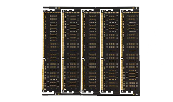
Key steps ensuring precision, reliability, and consistent multilayer PCB production quality.
Symmetric Stackup
Keep layers balanced to minimize board warpage.
Layer Count Planning
Allocate layers for signal, power, and ground planes carefully.
Microvia Placement
Place microvias strategically to reduce routing complexity.
Impedance Control
Critical for high-speed signals; use uniform layer thickness and dielectric spacing.
Thermal Management
Ensure power and ground planes are well-distributed to dissipate heat.
Manufacturability
Design within your manufacturer’s minimum drill size, aspect ratio, and lamination capability (Benlida supports 4-16+ layers with sequential lamination).
HDI PCB Testing and Quality Control
Benlida follows a comprehensive quality control system throughout the HDI PCB manufacturing process, from production monitoring to final inspection. With advanced testing equipment and strict quality procedures, Benlida ensures reliable performance, consistent quality, and long service life for HDI boards. As a professional HDI PCB supplier, Benlida is committed to providing products that meet customers’ requirements for precision and reliability.
Automated Optical Inspection (AOI)
During bare-board fabrication, AOI compares selected inner- or outer-layer circuit patterns with released image data. It identifies visible pattern deviations at the inspected stage. Electrical continuity and isolation are checked separately by electrical testing.
X-Ray Inspection
X-Ray inspection helps verify internal structures, including blind vias, buried vias, microvia connections, and multilayer alignment, ensuring the integrity and reliability of HDI structures.
Flying Probe Testing
Flying probe testing tests the electrical connections and helps to detect such problems as open circuits and shorts. This method is highly suitable for prototype testing.
PCBA ICT and Functional Testing
ICT and functional testing apply to assembled PCBA, not to an unpopulated PCB. ICT checks specified circuit nodes or component conditions through defined test access and fixtures. Functional testing runs the assembled unit against an approved procedure.
Manufacturing Process Monitoring
Benlida closely monitors critical manufacturing steps, including lamination, drilling, copper plating, and surface finishing. Continuous process control helps reduce variations and maintain consistent product quality.
Quality Standards and Reliability Management
All products are manufactured and inspected according to strict quality requirements, supported by IPC standards and ISO 9001 quality management practices to ensure every batch of HDI PCB delivers stable and reliable performance.
HDI PCB Applications Across Industries
Benlida provides reliable hdi boards for a wide range of industries where compact size, high circuit density, and stable performance are essential. As an experienced HDI PCB supplier, Benlida supports customers across different sectors with customized HDI solutions designed to meet various application requirements.
Consumer Electronics
HDI PCBs are widely used in smartphones, tablets, wearable devices, and other portable electronics that require lightweight designs, compact structures, and high component integration.
Automotive Electronics
With increasing demand for advanced vehicle systems, HDI technology helps support applications such as automotive control modules, infotainment systems, sensors, and other electronic components that require reliability and efficient space utilization.
Medical Equipment
Medical devices often require high precision and dependable performance. HDI boards provide compact and reliable circuit solutions for diagnostic equipment, monitoring devices, and portable medical electronics.
Communication Equipment
HDI PCBs support high-speed signal transmission and complex circuit designs in communication systems, networking equipment, and other applications that require stable electrical performance.
Industrial Electronics
Industrial control systems, automation equipment, and intelligent devices benefit from HDI technology due to its durability, high integration capability, and ability to support complex electronic designs.
Aerospace and High-End Electronics
For advanced electronic applications with strict requirements for reliability, size, and performance, HDI boards offer optimized interconnection structures and improved design flexibility.
FAQ
An HDI PCB uses high-density interconnect features, commonly laser-drilled microvias and sequential build-up layers, to route more connections within a limited board area. A conventional multilayer PCB may use plated through holes without an HDI build-up. Layer count alone does not define HDI; via structure, dielectric construction, pad geometry, and routing density must be reviewed together.
In common HDI notation, N commonly denotes the number of conductive layers in the central multilayer substructure, while the numbers indicate the build-up layers added to each side. 1+N+1 adds one build-up layer per side, and 2+N+2 adds two. The notation does not define via spans, stacked or staggered arrangements, drilling, fill or cap requirements, materials, or the lamination sequence; these details belong in the fabrication documentation.
A microvia dimension must state what is being measured, such as the design diameter, drilled diameter, entry or top diameter, bottom or target-side diameter, or finished diameter, as applicable. The fabrication documentation must also define the via depth or dielectric thickness, target- and capture-pad dimensions, copper construction, and any fill or cap requirement. A single minimum number without these conditions is incomplete.
Stacked microvias are vertically aligned through successive build-up layers; staggered microvias are offset from one layer to the next. The stack-up must identify each via span and arrangement. The selected structure depends on the interconnect path, routing space, pad geometry, dielectric construction, and fill or cap requirements.
For via-in-pad, identify the affected pads, via type, and layer span. State whether the via is open, filled, capped, and planarized, and define the fill material, void or dimple limits, surface finish, planarity, and finished-pad and assembly acceptance requirements. If a filled and plated-over structure is required, label it as VIPPO in the fabrication documentation.
HDI structures can support escape routing beneath a fine-pitch BGA, but manufacturability is specific to the design. Provide the package pitch, land pattern, pad stack, solder-mask geometry, microvia or via-in-pad structure, surface-finish and planarity requirements, and the escape-layer plan. Bare-board review does not establish SMT placement or assembly yield; a PCBA project requires a separate assembly review.
Provide the target impedance and tolerance, single-ended or differential definition, trace width and spacing, reference layers, proposed stack-up, material or Dk basis, copper thickness, and any coupon, test, or report requirement. Identify the controlled traces and relevant via transitions in the submitted fabrication data.
Specify the manufacturer and grade when required, together with the core, prepreg, or build-up dielectric construction, finished thickness, copper requirements, and applicable thermal or electrical properties. Include substitution rules in the procurement documentation. A broad label such as FR-4 or low-loss material is not a complete material specification.
Different methods provide different evidence. Process monitoring records defined fabrication parameters; AOI compares selected circuit patterns with released image data. X-ray can evaluate selected internal features within the resolution of the inspection setup, while finished bare-board netlist testing checks continuity and isolation. Microsection or agreed performance coupons can provide additional evidence for specified risks. The project plan defines the applicable item, method, stage, coverage or sampling, acceptance criteria, and records. ICT and functional testing apply to assembled PCBA, not to an unpopulated PCB.
IPC Class is a product performance and acceptance classification specified for an order; it is not a company certification. If an IPC class is required, the procurement documentation must identify the applicable standard, revision, class, customer amendments, acceptance criteria, and any required sampling, coupons, or records. The quotation and release must follow the requirements agreed for that project.
Provide current fabrication data, such as Gerber with NC Drill files or ODB++, plus a fabrication drawing and current revision. Include board dimensions, total layers, proposed build-up and via spans, material, finished thickness, copper, controlled-impedance requirements, surface finish, quantity, production stage, and requested schedule. Add the proposed stack-up, BGA or via-in-pad details, fill or cap requirements, customer specifications, acceptance criteria, and inspection or coupon requirements where applicable. If PCBA is included, submit the BOM, pick-and-place or centroid file, assembly drawing, sourcing approach, programming requirements, and test specification as a separate package.
Cost and lead time depend on the build-up and lamination cycles, microvia spans and arrangements, via filling, cap construction, and planarization, line and space, materials, controlled impedance, surface finish, panel utilization, quantity, inspection and documentation requirements, material availability, and the requested schedule. Price, MOQ, and lead time are confirmed after review of the complete fabrication package.
Prepare Your HDI PCB Data for Quotation
A complete fabrication package helps identify the board construction, unresolved technical questions, and the information still needed for quotation. Use the latest revision available. If the stack-up is not final, describe the routing, package, impedance, or space constraints and mark unknown items as “Not sure.”
Core PCB Quotation Information
- Current fabrication data, such as Gerber and NC drill files or ODB++ data
- Fabrication drawing and current revision
- Board dimensions, total layers, proposed build-up, and via spans
- Material, finished thickness, copper, and controlled-impedance requirements
- Surface finish, quantity, production stage, and requested schedule
Additional Information for Review
- Proposed stack-up and controlled-impedance table
- Microvia spans and stacked or staggered arrangements
- BGA land pattern and via-in-pad requirements
- Fill, cap, and planarization requirements
- Customer specifications and requested acceptance criteria
- Panel or mechanical drawing, special tolerances, and inspection or coupon requirements
If PCBA Is Included
If PCBA is also required, provide the BOM, pick-and-place or centroid file, assembly drawing, sourcing approach, programming requirements, and test specification as a separate assembly package. PCBA test requirements are separate from bare-board electrical test requirements.
Use this checklist to prepare the current revision of your fabrication package, together with the technical, quantity, and schedule information needed for review. Confirm the accepted transfer method and file requirements before sending confidential design data.