

PCB Assembly Services
PCB Assembly Services from Prototype to Production
Reliable PCB assembly service provider delivering high-quality SMT, THT, and complete PCBA manufacturing solutions. Providing flexible, one-stop turnkey PCB assembly solutions for global electronics manufacturers, covering everything from procurement, assembly, and testing to delivery.
Need bare PCBs before assembly? View our PCB Manufacturing Services for board types, manufacturing requirements, and project-specific fabrication options.
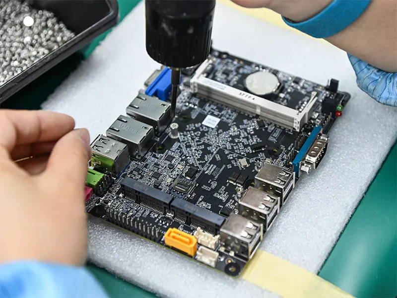
PCB Assembly Types We Offer
Complete Spectrum PCB Assembly, Designed for Excellence
Our complete range of PCB assembly services caters to diverse production needs, ranging from prototypes and low-volume production to mass production. Using sophisticated machinery and stringent quality standards, we offer customizable assembly services for multiple industries.
SMT Assembly
SMT assembly places surface-mount components on the manufactured bare PCB according to the released placement data. Once the components are assembled, the populated board is a PCBA. Applicable packages, process routing, and inspection requirements are confirmed for each project. For process-specific details, see our SMT assembly services.
THT Assembly
THT assembly inserts component leads through plated holes in the manufactured bare PCB and solders them on the opposite side. Once the components are assembled, the populated board is a PCBA. The applicable soldering method and inspection requirements are confirmed for each project. For process-specific details, see our through-hole and DIP assembly services.
Mixed/Hybrid Assembly
Mixed assembly combines SMT and THT on the same PCB. This solution is ideally suited for complex circuit boards, particularly those requiring a combination of compact, precision components and rugged, durable parts.
Prototype & Small-Batch Assembly
Assembly solutions provide support for product development, engineering validation, and prototyping. The advantage of this service is that it allows the customer to verify the design before going into large-scale production.
Turnkey PCB Assembly
Turnkey PCB assembly offers a manufacturing solution that covers everything from component sourcing through PCB assembly and testing to delivery. This service helps customers optimize supply chain management.
High-Volume Production
Large-scale manufacturing capacity enables high-volume production with good product quality, consistent delivery performance, and effective production management.
Benlida PCB Assembly Capabilities
From Prototype to Mass Production – Advanced Manufacturing
Experience the benefits of a state-of-the-art manufacturing setting where precision, efficiency, and quality control are integrated. With professional production equipment and strict quality inspections, our PCB assembly process guarantees reliable performance at each manufacturing stage. From initial design evaluation to final product delivery, we provide turnkey PCB assembly services, helping customers manage the entire production process with greater efficiency and reliability.
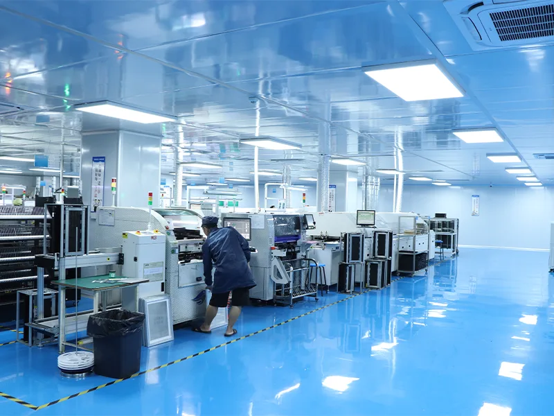
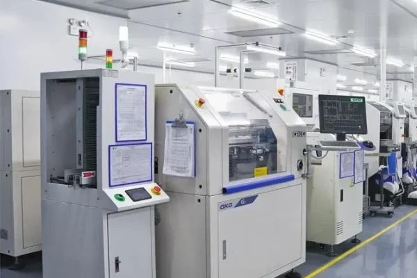
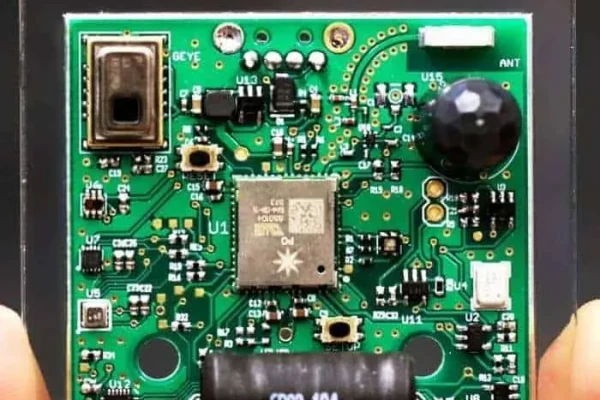
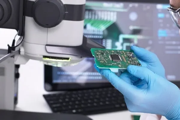
Prototype & Low-Volume Assembly
Engineering-focused assembly builds for design validation, testing, and early production.
SMT, THT & Mixed Assembly
Surface-mount, through-hole, and mixed-technology assembly for different project requirements.
Production PCB Assembly
Repeat and scheduled assembly builds based on approved BOMs, placement data, and process requirements.
Turnkey & Consigned Assembly
Turnkey, partial-turnkey, and consigned options for component sourcing and assembly.
PCB Assembly Process
The production route is defined for each project from the released build data, component mix, sourcing responsibilities, assembly method, and agreed inspection, programming, and test requirements. The stages below form a conditional project map; a stage may be omitted, repeated, or sequenced differently when the approved process route requires it.
Before the affected work is released, identify the current revisions of the PCB, BOM, placement and assembly data, together with the sourcing model and any applicable programming, inspection, or test requirements.
Prepare the components and bare PCBs required for the released assembly build under the agreed sourcing model. Bare PCB fabrication remains a separate scope; any incoming checks and acceptance criteria are defined for the project.
For applicable SMT builds, solder paste is printed before placement. SPI is a separate inspection option and is used only when it is included in the agreed inspection plan and supported by defined criteria.
For a reflow-based SMT route, surface-mount components are placed from the released placement data and soldered through the specified reflow process. The sequence depends on the component mix and approved process route.
AOI may inspect visible component placement and solder features at defined process points. X-Ray may be used for solder features hidden from optical inspection. Method, coverage, and acceptance criteria are defined for the project.
For THT or mixed-technology builds, through-hole components are inserted and soldered using the method defined for the project. The sequence, soldering method, process conditions, and inspection criteria depend on the assembly design and agreed route.
Programming, ICT, and functional testing are separate options and may occur at different process points. Include only the methods stated in the agreed scope and supported by the required approved files, test access, fixtures, procedures, operating conditions, limits, and responsibility split.
Burn-In is not a default assembly step. When it is specified and supported, define the units, operating mode or load, environmental conditions, duration, monitoring, acceptance criteria, and reporting requirements before release. Burn-In should not be presented as proof of service life or reliability unless the approved protocol supports that conclusion.
The final stage covers the inspection, labeling, traceability records, and packaging activities agreed for the project before release for shipment. Acceptance criteria, traceability fields, record scope, and packaging requirements are project-defined.
Cleaning and Rework Verification When Applicable
Cleaning depends on the flux chemistry, soldering materials, assembly design, component compatibility, process, and cleanliness criteria. When authorized rework is performed, the affected area and any impacted function are reinspected or retested against the project-defined acceptance criteria.
Start Your PCB Assembly Project
Submit your Gerber or ODB++ files, BOM, centroid data, assembly drawing, quantity, revision, sourcing model, and testing or programming requirements. Our team will review the PCBA scope and prepare a project-specific quotation for prototype or production assembly.
What Is PCB Assembly?
PCB manufacturing produces an unpopulated bare board. PCB assembly mounts and solders electronic components onto that board to create a printed circuit board assembly (PCBA). These are separate production scopes and require different project data.
A bare PCB quotation requires fabrication data and board requirements. A PCBA quotation additionally requires a BOM, pick-and-place or centroid data, assembly drawings, the sourcing model, and any applicable firmware or test requirements.
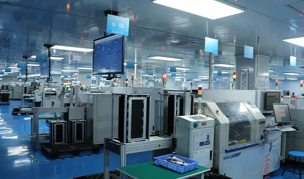
PCB Assembly Support Across Industries
Consumer Electronics
PCB assembly support for consumer electronics projects, from prototype builds to scheduled production, based on the approved BOM, placement data, and test requirements.
Industrial Automation
PCB assembly support for industrial controllers, sensors, and automation equipment, with project-defined inspection, functional testing, and traceability requirements.
Medical Devices
PCB assembly support for medical electronics projects based on customer drawings, applicable specifications, and an agreed inspection and test plan.
Automotive Electronics
PCB assembly support for automotive electronics projects based on customer specifications, approved materials, and project-defined inspection and test requirements.
Telecommunications
PCB assembly support for networking and communication equipment, with component sourcing, assembly, inspection, and functional testing defined for each project.
Aerospace Electronics
PCB assembly support for aerospace electronics projects is reviewed against customer drawings, contractual requirements, approved materials, and an agreed inspection and test plan.
Why Choose Benlida for PCB Assembly?
Trustworthy PCB Assembly Manufacturing Company to Meet Your Requirements
Choosing the right manufacturing partner is important for maintaining product quality, delivery efficiency, and production stability. With professional experience and advanced production capabilities, Benlida provides comprehensive PCBA solutions from prototypes to large-scale manufacturing.
Flexible production planning supports:
● Prototype assembly
● Small-batch production
● Urgent manufacturing requirements
● Large-scale orders
This allows customers to bring electronic products to market faster.
● AOI inspection
● X-ray inspection
● Electrical testing
● Functional testing
These inspection and testing methods ensure reliable performance for every turnkey PCB assembly project.
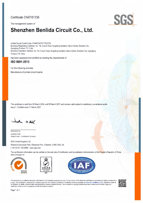
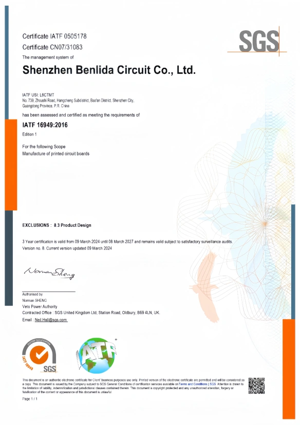
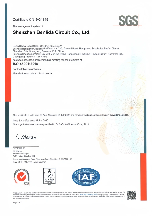
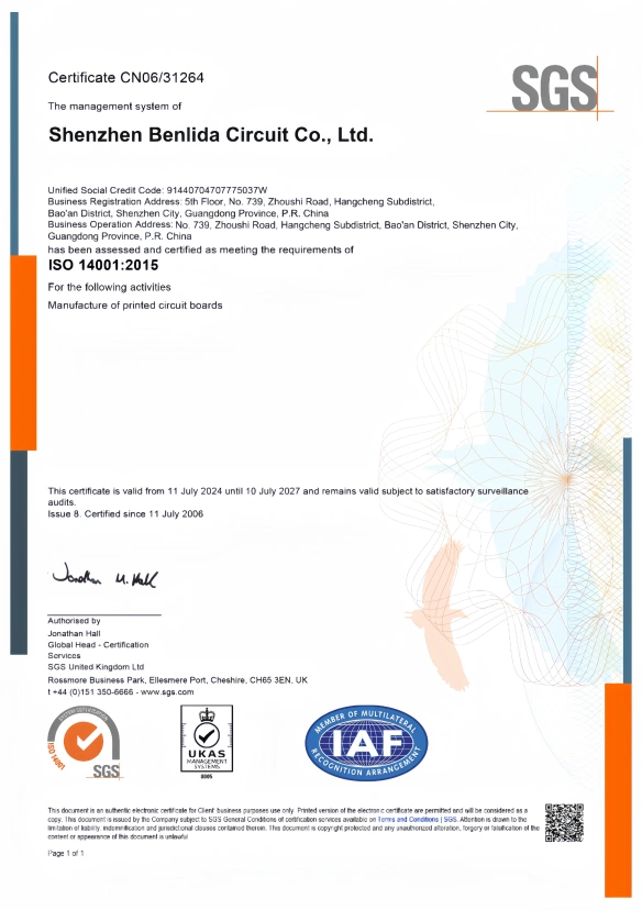
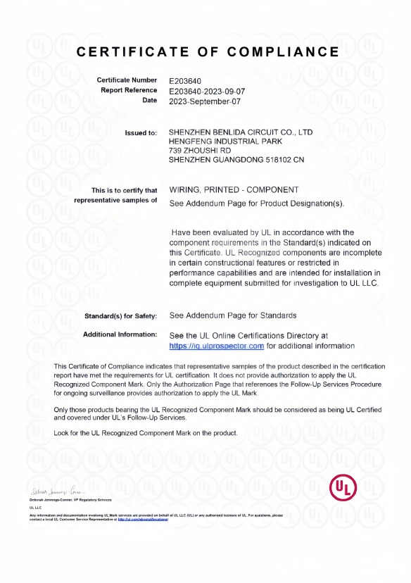
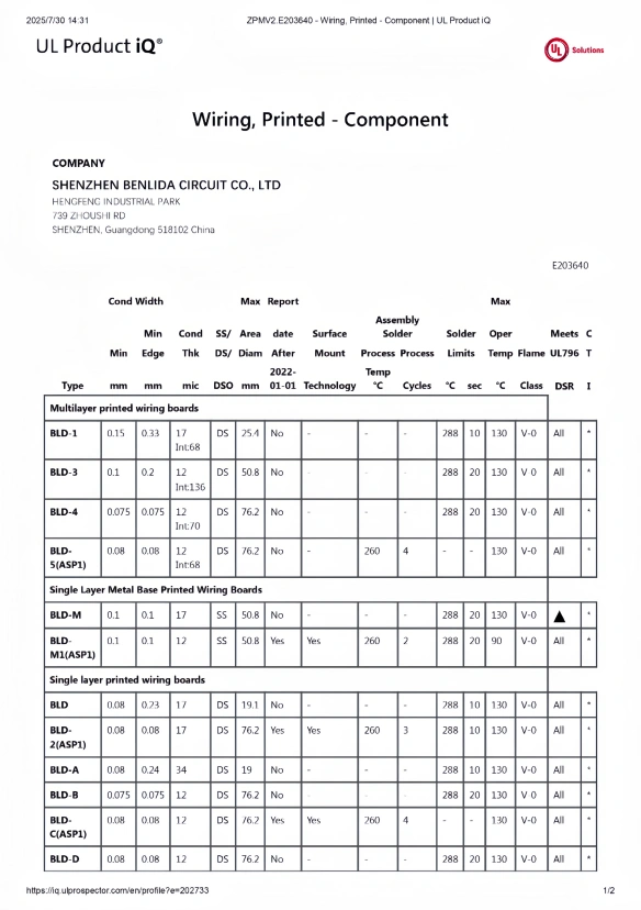
Our Certificates
Quality Certifications Supporting Reliable Manufacturing
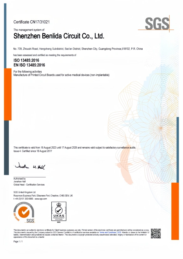
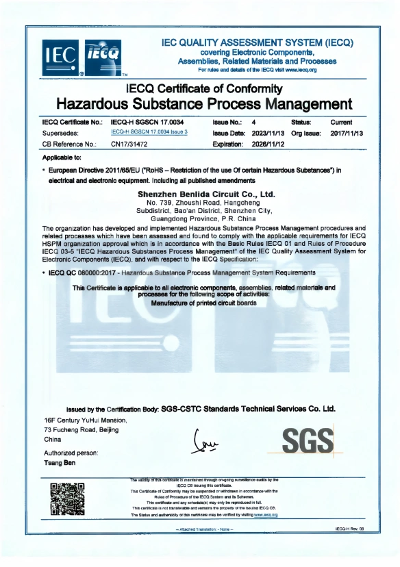
Benlida is committed to maintaining high manufacturing standards through strict quality management systems. Professional certifications demonstrate continuous improvement in production control, product reliability, and environmental responsibility.
Our certificates include internationally recognized certifications such as SGS verification, supporting reliable PCB manufacturing and assembly services for global customers.
PCB Assembly Inspection, Testing and Programming Options
Inspection, testing, and firmware programming are separate, project-defined PCBA activities. SPI, AOI, and X-Ray inspect process or assembly conditions; they do not confirm powered function. ICT, functional testing, firmware flashing, and Burn-In are included only when specified and confirmed for the project.
The applicable method, coverage, sampling, access, fixtures, programs, software, pass/fail limits, records, and responsibilities depend on the released project data and agreed scope. No single method proves that a PCBA is free from every possible defect.
For the broader inspection and control framework, see our PCB and PCBA quality control page.
Assembly Inspection
Solder Paste Inspection (SPI)
Purpose: SPI may inspect deposited solder paste before component placement when SPI is included in the approved process route.
Project Inputs: Approved print setup, inspection program, coverage or sampling, and acceptance criteria.
Limits: SPI does not inspect completed solder joints or confirm electrical function.
Automated Optical Inspection (AOI)
Purpose: AOI may inspect optically visible component placement, orientation, and soldering conditions, such as missing, shifted, or incorrectly oriented parts.
Project Inputs: Inspection program, visible features, coverage or sampling, and acceptance criteria.
Limits: Coverage depends on optical access, component geometry, equipment configuration, and the agreed inspection plan. AOI does not confirm electrical function.
X-Ray Inspection
Purpose: X-Ray may examine selected solder structures that are not fully visible from the surface.
Project Inputs: Target areas, inspection setup, coverage or sampling, and acceptance criteria.
Limits: X-Ray cannot reveal every assembly defect or confirm electrical function.
Electrical and Functional Testing
In-Circuit Testing (ICT)
Purpose: ICT may check selected accessible nets and components for agreed electrical conditions.
Project Inputs: DFT and test-point access, fixture, program, limits, and required coverage.
Limits: Applicability and coverage are project-specific. ICT does not replace functional testing.
Functional Testing
Purpose: Functional testing evaluates powered PCBA behavior against an agreed procedure and pass/fail criteria. Depending on the project, it may cover selected inputs, outputs, interfaces, communications, or operating functions.
Project Inputs: Fixtures, firmware when required, power and signal conditions, loads, responsibilities, and expected results.
Limits: Functional testing verifies only the functions and conditions included in the agreed test scope.
For detailed test inputs and fixture requirements, see our PCBA functional testing service.
Burn-In When Specified
Purpose: Burn-In may involve operating the PCBA or assembled product under defined conditions for a specified period when required.
Project Inputs: Power, load, temperature or environmental conditions, duration, monitoring, quantity or sampling, records, and pass/fail criteria.
Limits: Burn-In is not a guarantee of service life or freedom from latent defects.
Firmware Programming
Firmware Flashing
Purpose: Firmware flashing may load an approved file and version into a specified target device.
Project Inputs: Target device, programming interface or fixture, instructions, device state, security requirements, and verification method.
Limits: Configuration, calibration, serialization, power-up checks, and functional testing are separate unless expressly included in the agreed scope.
For device, file, and verification requirements, see our firmware flashing services.
FAQ
PCB assembly covers SMT, THT, or mixed assembly. Depending on the project, component sourcing, bare-PCB supply, firmware flashing, inspection, testing, and packaging can also be included.
In turnkey assembly, the supplier sources the components. In partial-turnkey assembly, the customer supplies selected parts and the supplier sources the remainder. In consigned assembly, the customer supplies the assembly components. The quotation records the responsibility for PCBs and components.
For a PCBA quotation, provide Gerber or ODB++ data, a BOM with manufacturer part numbers, Pick-and-Place or Centroid data, assembly drawings, quantity, revision, and the sourcing model. Add firmware and test requirements when needed.
A PCB is an unpopulated printed board. A PCBA is the board after electronic components have been mounted and interconnected. PCB fabrication and PCB assembly are separate production scopes.
Before a production or repeat build, confirm that the PCB data, BOM, placement data, assembly drawings, firmware, test files, quantity, and acceptance criteria use the same released revision. Prototype results alone do not authorize production release.
SPI checks solder-paste deposits; AOI checks visible placement and soldering features; X-Ray examines selected hidden solder structures. ICT checks accessible electrical conditions, while functional testing evaluates defined powered functions. Burn-In is a separate operating screen, and firmware flashing is programming. The project design and test requirements determine the applicable combination.
Firmware flashing can be included with an approved file and version, target device and board revision, programming interface or fixture, instructions, and verification method. Functional testing is defined separately.
No. DFM and DFA reviews focus on manufacturability and assembly. Circuit function, firmware, product safety, and finished-product performance require separate verification.
List approved manufacturer part numbers, approved alternatives, and the required approver in the BOM or RFQ package. Any proposed substitute is reviewed for fit, function, package, lifecycle, sourcing, and test impact before approval.
Provide the approved test procedure, power and signal conditions, loads, expected inputs and outputs, pass/fail limits, firmware version, interfaces, fixtures, required records, and responsibility for test hardware and software.