

Custom Ceramic PCB Manufacturing
Discuss your ceramic circuit board requirements with Benlida. Define the ceramic material, metallization process, copper geometry and inspection requirements for your project.
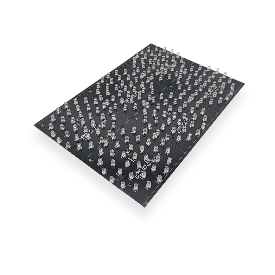
What Is a Ceramic PCB?
A ceramic PCB is a circuit board that is made using ceramic materials for its substrate instead of the common FR-4 material. It is usually designed for electronic applications that have the need for efficient thermal management, high electrical properties, and reliability. Ceramic PCBs are distinguished by their increased heat conduction, heat-resistance, and dimensional stability, hence, they are the perfect choice in cases of dealing with heat produced by high-power electronic parts.
Several types of ceramic materials can be employed for producing ceramic PCBs, like alumina (Al2O3) and aluminum nitride (AlN). AlN PCB is one of the most widespread types of ceramic PCBs and is also called aluminum nitride PCB or AlN PCB. Due to its great ability of heat dissipation and insulation, AlN PCB is commonly used in such applications as power modules, LED lighting, semiconductor packaging, RF devices and high reliability electronics.
Related services and board types: Explore our PCB Manufacturing Services.
What Is a Ceramic PCB?
A ceramic PCB is a circuit board that is made using ceramic materials for its substrate instead of the common FR-4 material. It is usually designed for electronic applications that have the need for efficient thermal management, high electrical properties, and reliability. Ceramic PCBs are distinguished by their increased heat conduction, heat-resistance, and dimensional stability, hence, they are the perfect choice in cases of dealing with heat produced by high-power electronic parts.
Several types of ceramic materials can be employed for producing ceramic PCBs, like alumina (Al2O3) and aluminum nitride (AlN). AlN PCB is one of the most widespread types of ceramic PCBs and is also called aluminum nitride PCB or AlN PCB. Due to its great ability of heat dissipation and insulation, AlN PCB is commonly used in such applications as power modules, LED lighting, semiconductor packaging, RF devices and high reliability electronics.
Related services and board types: Explore our PCB Manufacturing Services.
Choose a Ceramic Material for Your Requirements
The performance of a ceramic printed circuit board mainly depends on the type of ceramic substrate employed in the manufacturing process. Each ceramic has its own characteristics that can be exploited in different ways during the production of the printed circuit board. Benlida has a range of ceramic printed circuit boards which make use of ceramics such as Al₂O₃, AlN, Si₃N₄, and more.
| Selection point | Alumina (Al₂O₃) | Aluminum nitride (AlN) | Silicon nitride (Si₃N₄) |
|---|---|---|---|
| Material focus | Consider when balancing insulation, thermal needs and cost. | Consider when heat conduction is a key design requirement. | Consider when mechanical demands and thermal cycling are central to the design. |
| Data to compare | Grade-specific thermal, electrical and mechanical data. | Grade-specific thermal conductivity, expansion and electrical data. | Grade-specific strength, fracture toughness and thermal data. |
| Design trade-off | Check whether the complete heat path meets the target temperature. | Evaluate the thermal benefit alongside thickness, interfaces and cost. | Evaluate mechanical behavior alongside copper structure and assembly loads. |
| Process compatibility | Confirm the grade and surface condition for the selected route. | Confirm the grade and surface condition for the selected route. | Confirm the grade and surface condition for the selected route. |
| Required inquiry inputs | Heat load, insulation needs, dimensions, mounting and quantity. | Heat load, insulation needs, dimensions, mounting and quantity. | Heat load, insulation needs, dimensions, mounting and quantity. |
DPC, DBC and AMB Process Options
DPC, DBC and AMB use different methods to form or attach copper on a ceramic substrate. They should not be treated as interchangeable options with one shared set of manufacturing limits.
DPC uses a metallization and plating route to build copper patterns. DBC joins copper to a ceramic surface through a bonding process. AMB uses active brazing materials to join metal and ceramic. Each route needs its own material compatibility, copper geometry and inspection requirements.
Confirm the proposed material and process combination before finalizing your design. Fine circuit features, thick copper and demanding reliability requirements must be assessed together.
Compare Metallization Routes
| Comparison point | DPC (Direct Plated Copper) | DBC (Direct Bonded Copper) | AMB (Active Metal Brazing) |
|---|---|---|---|
| How copper is formed or joined | Metallization and plating build the copper layers. | A bonding process joins copper to a prepared ceramic surface. | Active brazing materials join metal and ceramic. |
| Material compatibility | Confirm the ceramic grade and surface preparation. | Confirm the ceramic grade and required surface condition. | Confirm the ceramic grade and brazing system. |
| Geometry to review | Finished copper thickness, pattern dimensions and any interconnect features. | Copper thickness, etched geometry and ceramic-to-copper structure. | Copper structure, brazed interfaces and pattern dimensions. |
| Inspection focus | Copper thickness, circuit geometry and adhesion requirements. | Interface quality, copper geometry and agreed electrical checks. | Brazed interface quality and the agreed mechanical and electrical checks. |
| Project decision | Assess the proposed material and route against the complete drawing. | Assess the proposed material and route against the complete drawing. | Assess the proposed material and route against the complete drawing. |
Ceramic PCB Manufacturing Capabilities
Considering that the manufacturing process of the PCB would impact its performance and efficiency, we at Benlida, a professional ceramic PCB manufacturer,provide you with the most advanced ceramic PCB technology like DPC, DBC, AMB, etc. along with the advanced material of aluminum nitride PCB.
Ceramic PCB Technical Capability Parameters
| Technical Item | Capability Range |
|---|---|
| Ceramic Materials | Alumina , Aluminum Nitride , Silicon Nitride |
| Ceramic PCB Thickness | 0.2mm - 3.0mm (custom options available) |
| Copper Thickness | 10μm - 300μm |
| Maximum Panel Size | Customized according to process requirements and product design |
| Minimum Line Width / Spacing | 0.075mm / 0.075mm (depending on manufacturing process) |
| Thermal Conductivity | Al₂O₃: 20-30 W/(m·K), AlN: 140-180 W/(m·K), Si₃N₄: 80-100 W/(m·K) |
| Surface Finish | ENIG, OSP, Gold Plating, and other finishes |
| Metallization Processes | DPC, DBC, AMB |
| Operating Temperature | Suitable for high-temperature applications based on material selection and design requirements |
| Application Capability | High-power electronics, LED modules, semiconductor packaging, automotive electronics, and more |
Ceramic PCB Applications
The ceramic PCB is extensively employed in electronic devices that need excellent heat management and electrical insulation properties. Being a professional ceramic PCB manufacturer, Benlida offers ceramic circuit board products based on various materials such as alumina and aluminum nitride PCBs.
Power Electronics
Being characterized by high heat dissipation efficiency, ceramic PCBs are widely applied in power modules, IGBT modules, power supplies, and high-current electronic equipment.
LED Lighting and High-Power LED Modules
LED elements have high heat dissipation requirements; therefore, thermal management is crucial for ensuring product functionality and its service life. Ceramic circuit boards are extensively employed in high-power LEDs, UV LEDs, and other specific lighting fixtures.
Semiconductor Packaging and Chip Applications
Ceramic substrates are characterized by stable heat properties and reliable insulation; therefore, they can be utilized in semiconductor packaging, chip carriers, and other complex electronic modules.
Automotive Electronics
The increasing demand for electric vehicles and intelligent automotive systems requires electronic components with improved heat dissipation and reliability. Ceramic PCBs are used in applications such as EV power modules, motor control systems, battery management systems (BMS), and other automotive electronics.
RF and High-Frequency Electronics
Ceramics possess stable electrical properties and superior performance at high frequencies. The use of ceramic PCB is suitable for RF modules, communication devices, microwave circuits, and other electronic equipment operating at high frequencies.
Aerospace and High-Reliability Equipment
For applications in aerospace, industrial control, and other such tough conditions, there should be stability in functioning over an extended period of time.Ceramic PCB possesses high thermal resistance, mechanical stability, and reliability for extreme environments.
Why Choose Benlida: Manufacturing Advantages and Quality Control
As an experienced ceramic PCB manufacturer, Benlida pays much attention to the provision of reliable ceramic PCB products with excellent manufacturing capability and rigorous quality control.
Extensive Ceramic PCB Manufacturing Experience
Benlida has experience in ceramic circuit board production and understands the characteristics of different ceramic materials, including alumina (Al₂O₃) and aluminum nitride PCB. We provide suitable material and process recommendations based on different application requirements.
Multiple Ceramic PCB Process Capabilities
With support for advanced metallization processes such as DPC, DBC, and AMB, Benlida can manufacture ceramic PCBs with different requirements for thermal performance, circuit precision, and reliability, suitable for high-power and high-stability electronic applications.
Customized Manufacturing Support
Benlida gives flexible customization possibilities to customers of ceramic PCB products in terms of substrate material, size, copper thickness, circuitry design, and surface finish. It gives customers an opportunity to create a more appropriate solution for their needs.
Strict Quality Control System
Quality control is performed throughout the whole production process – starting from material control, manufacturing process control, and ending with finished product control.
Technical Support and Fast Response
Benlida provides engineering assistance to its customers with respect to product selection, process optimization, and technical communication for successful project implementation and stable delivery.
Inspection and Quality Verification
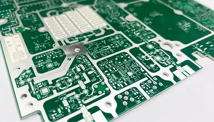
To ensure the performance and reliability of each ceramic PCB, Benlida applies strict inspection procedures throughout the manufacturing process. As an experienced ceramic PCB manufacturer, we perform material verification, process monitoring, and final testing to ensure products meet the requirements of high-reliability electronic applications.
Material Inspection
Before production, ceramic substrate materials are carefully inspected to ensure they meet design and application requirements. Materials such as alumina (Al₂O₃) and aluminum nitride PCB substrates are verified for consistency and quality.
Inspection items include:
• Material specification verification
• Visual inspection
• Thickness measurement
• Material consistency evaluation
Dimensional Inspection
Since precise dimensions are vital in the assembly and functionality of Ceramic PCBs, it is important that key dimensions be checked during the manufacturing process as per customer specifications.
Inspection items include:
• PCB dimensions
• Board thickness
• Hole size and position accuracy
• Circuit pattern dimensions
Copper Layer and Bonding Inspection
For ceramic PCB processes such as DPC, DBC, and AMB, the bonding quality between ceramic substrates and copper layers is carefully inspected to ensure strong adhesion and long-term stability.
Inspection items include:
• Copper thickness measurement
• Bonding strength evaluation
• Surface quality inspection
Electrical Performance Testing
Electrical testing is performed to verify insulation performance and circuit reliability, ensuring stable operation under different working conditions.
Inspection items include:
• Insulation resistance testing
• Dielectric withstand testing
• Electrical continuity testing
Thermal Performance Testing
Thermal performance is one of the major strengths of ceramic PCB, particularly in power applications. The thermal performance test ensures the ability of heat dissipation in the product.
Inspection items include:
• Thermal conductivity testing
• Thermal performance evaluation
• High-temperature testing
Reliability Testing
For applications requiring long-term stability, ceramic PCBs undergo reliability testing to evaluate performance under demanding operating environments.
Inspection items include:
• Thermal cycling testing
• High-temperature aging testing
• Environmental reliability testing
Ceramic PCB Manufacturing FAQs
A ceramic PCB uses a ceramic substrate to support the circuit. A metal-core PCB uses a metal base with an insulating layer between the base and the circuit. Compare the complete structure, heat path and electrical requirements when choosing between them.
Start with your thermal, electrical, mechanical and cost requirements. Compare the data for the actual material grades, then review substrate thickness, copper geometry and assembly conditions. The material name alone is not a complete specification.
DPC builds copper through metallization and plating. DBC bonds copper to a prepared ceramic surface. AMB uses active brazing materials to join metal and ceramic. Their material compatibility and manufacturing limits need to be assessed separately.
The available combination needs to be confirmed for your specification. Include the preferred material, ceramic and copper thicknesses, circuit dimensions and inspection requirements in your inquiry. Ask for a quotation that identifies the accepted manufacturing configuration.
Copper thickness, line width and spacing must be reviewed together. The manufacturing route and the way finished dimensions are measured also matter. A minimum line dimension listed without its copper thickness should not be treated as valid for every design.
No. Material thermal conductivity is only one part of the heat path. Ceramic thickness, heat-source size, connection layers, mounting interfaces and the cooling arrangement also affect temperature. Compare designs under the same operating and test conditions.
These features require confirmation for the selected material and process. Specify the circuit and copper on each side, the hole type and dimensions, and whether electrical connection or filling is required. A drilled or laser-cut hole does not by itself establish a metallized interconnect.
Choose the finish for the intended attachment method. Include the required metal system, layer thickness and surface conditions where specified. Gold plating alone does not establish wire-bonding compatibility; the finish and bonding process need to be evaluated together.
The inspection scope must be stated in the quotation or agreed specification. Distinguish routine checks from sampling, qualification and project-specific testing. Ask which records can be provided and whether additional tests require a separate cost or schedule.
Share the application, approximate dimensions, quantity and any known material or thickness requirements. You can describe requirements that are still undecided. A manufacturing quotation will need more detail, including the drawing revision, circuit geometry, finish, tolerances and inspection scope. Confirm accepted file formats before sending production files.
State the delivery level you need in your inquiry. Bare metallized substrates, SMT assemblies, die attachment and wire bonding are different scopes and require separate confirmation. A BOM is relevant to assembly work; it is not automatically required for a bare-substrate inquiry.
Material availability, the manufacturing route, dimensions, copper geometry, finish, quantity and inspection requirements can all affect cost and schedule. Drawing approval, special tests and shipping also need to be considered. Confirm MOQ, production timing and any separate engineering or tooling charges in the quotation.
Discuss Your Ceramic PCB Project
For an initial inquiry, share your application, approximate dimensions, expected quantity and contact details. If the material, process or drawings are not final, explain what is known and which requirements still need review.
For a manufacturing quotation, include the drawing revision, material specification, ceramic and copper thicknesses, circuit geometry, surface finish, tolerances and inspection requirements. State whether you need single pieces or panels and give your requested delivery date.
Confirm the accepted file formats and transfer method before sending production files. BOM and assembly data are relevant only when additional assembly work is part of the agreed scope.