Reflow Soldering Defects — Causes, How to Prevent Them & Fix Guide
Reflow soldering defects can reduce yield, increase rework, and cause field failures. Some defects are easy to see. Others remain hidden under a BGA or QFN package. A defect may come from the reflow profile, but the profile is not always the only cause. Solder paste printing, PCB pad design, component placement, storage, and material condition also matter.
This guide explains five common SMT soldering defects. You will learn how to identify each defect, find its likely root cause, and choose a practical corrective action. The goal is not to change every process setting at once. The goal is to use evidence and adjust one variable at a time.
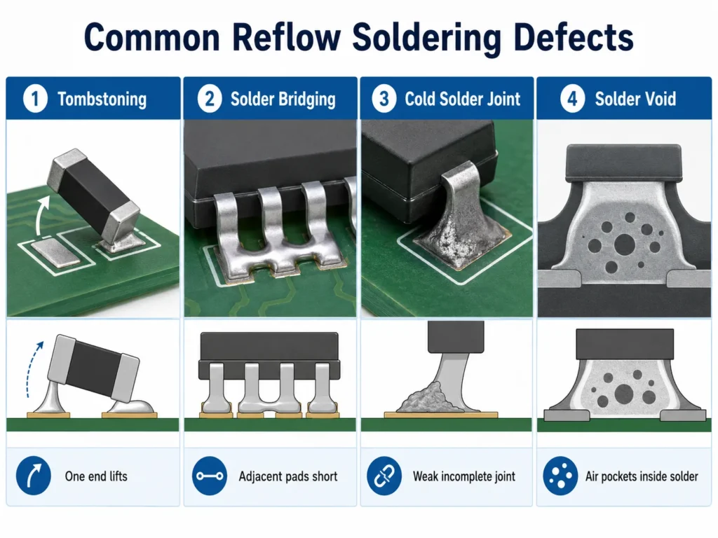
Common reflow soldering defects include tombstoning, bridging, cold joints, voids, and head-in-pillow.
What Causes Reflow Soldering Defects?
A reflow defect develops when heat, materials, printing, or placement move outside the process window. The root cause may begin before the PCB enters the oven.
An incorrect reflow profile
The PCB must heat at a controlled rate. Heating too fast can boil flux or cause paste slump. Heating too slowly can exhaust the flux. Uneven heating also creates temperature differences across the board.
Poor solder paste printing
Many SMT defects begin at the stencil printer. Too much paste can cause bridging. Too little paste can cause opens or weak joints. Blocked apertures can create uneven deposits.
Pad or stencil design problems
Unequal pads can create unbalanced wetting forces. Large apertures deposit too much paste. Very small apertures may release paste poorly. Stencil design must match component pitch and pad size.
Placement errors
An offset, rotated, or over-pressed component may not form balanced joints. Incorrect placement can increase tombstoning, bridging, and area-array opens.
Oxidation or contamination
Oxides, dust, oil, moisture, and expired materials can prevent wetting. Contamination may affect pads, terminations, solder powder, or handling surfaces. More heat cannot always solve poor solderability.
| Defect | Typical appearance | Common causes | First checks |
|---|---|---|---|
| Tombstoning | One end of a passive component lifts | Uneven heating, unequal paste deposits, pad mismatch | Pad temperatures, print balance, placement |
| Solder bridging | Solder connects adjacent pads or leads | Excess paste, paste slump, large apertures, placement offset | Stencil, paste volume, print alignment |
| Cold solder joint | Dull, rough, weak, or poorly wetted joint | Insufficient heat, oxidation, contamination, low paste activity | Peak temperature, time above liquidus, solderability |
| Solder voids | Gas pockets inside the joint | Flux outgassing, trapped volatiles, pad design, paste volume | X-ray image, stencil design, profile, via-in-pad |
| Head-in-pillow | BGA ball and paste touch but do not merge | Package warpage, oxidation, poor paste transfer | X-ray, paste deposit, BGA warpage, profile |
These defects are easier to control when printing, placement, reflow, and inspection are managed as one process. Learn more about Benlida’s SMT assembly services.
Tombstoning — Cause and Prevention
Tombstoning happens when one end of a small passive component lifts from the PCB. The component may stand vertically or at a steep angle. This defect is common on small resistors and capacitors.
The main mechanism is unbalanced wetting force. One solder deposit melts and wets before the other. Its surface tension pulls one side of the component downward. The opposite side then rises.
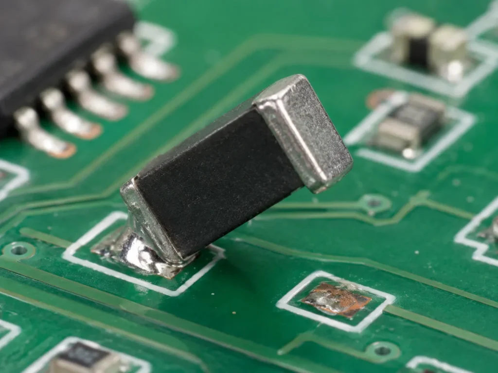
A tombstoning PCB defect forms when wetting forces are not balanced at both ends of the component.
Common causes of tombstoning
- One pad heats faster than the other.
- One pad is connected to a large copper area or ground plane.
- Pad sizes or solder mask openings are not symmetrical.
- Solder paste deposits have different volumes.
- The component is placed off-center.
- The ramp rate is too fast for the board design.
How to prevent tombstoning
- Use symmetrical pads and balanced thermal connections.
- Check stencil aperture size and paste transfer on both pads.
- Improve placement centering and component release.
- Reduce the temperature difference between the two pads.
- Test a controlled ramp or a short soak below the alloy melting point.
- Confirm that the paste is stored, thawed, and mixed correctly.
Do not add a long soak without testing. A long soak can consume flux activity and increase oxidation. It may solve one defect while creating another.
Solder Bridging — Cause and Prevention
A solder bridge defect is an unwanted solder connection between adjacent pads, pins, or leads. It can create an electrical short. Fine-pitch ICs are especially sensitive because the spacing is small.
Common causes of solder bridging
- Too much solder paste is printed.
- The stencil is too thick for the component pitch.
- Stencil apertures are too large or poorly designed.
- The solder paste slumps before reflow.
- The PCB and stencil are not aligned.
- The component is placed off-center.
- The preheat ramp is too aggressive.
How to prevent solder bridging
- Reduce aperture area where excessive paste is confirmed.
- Use a stencil thickness that suits the smallest pitch on the board.
- Inspect print height, area, and volume with solder paste inspection.
- Clean the stencil underside at a controlled interval.
- Verify board support to prevent PCB movement during printing.
- Correct placement offsets before changing the oven settings.
- Use a controlled heating rate to limit paste slump and spattering.
When bridging appears on many boards in the same location, first inspect the stencil and pad design. When it appears randomly, check paste condition, stencil cleaning, board support, and placement stability.
Cold Solder Joints — Cause and Prevention
A cold solder joint may look dull, grainy, cracked, or poorly wetted. The joint may have weak mechanical strength or unstable electrical performance. However, visual appearance alone is not enough for every alloy. Some lead-free joints naturally look less shiny than traditional tin-lead joints.
Common causes of a cold solder joint
- The joint does not reach the required peak temperature.
- Time above liquidus is too short.
- A heavy component or copper area remains cooler than the rest of the board.
- PCB pads or component leads are oxidized.
- Flux activity is too low or has been exhausted.
- Solder paste is expired, dry, or handled incorrectly.
- The surfaces contain oil, dust, or other contamination.
How to prevent cold solder joints
- Profile the actual production board, not an empty conveyor.
- Attach thermocouples to the coldest and most critical joints.
- Confirm peak temperature and time above liquidus against the paste data sheet.
- Check PCB finish and component termination solderability.
- Control solder paste storage, thawing time, and stencil life.
- Keep handling surfaces clean and dry.
If only one component type shows poor wetting, investigate the component finish and storage history. If many locations are affected, review the paste, profile, and board surface condition.
Consistent printing, placement, material control, and thermal profiling must work together. Benlida applies these controls throughout its PCB assembly services.
Solder Voids — Cause and Prevention
Solder voids are gas pockets trapped inside a solder joint. They are common under QFN thermal pads, BGAs, LGAs, and other bottom-terminated components. Voids are usually evaluated with X-ray inspection because they cannot be seen from the outside.
Common causes of solder voids
- Flux volatiles cannot escape before the solder solidifies.
- Too much paste or an unsuitable aperture pattern traps gas.
- Too little paste creates solder starvation at the pad.
- Via-in-pad structures provide paths that affect solder flow.
- Oxidation reduces wetting and traps residue.
- The profile is too long, too short, too hot, or poorly matched to the paste.
How to reduce solder voids
- eview the void location, size, and shape in the X-ray image.
- Use a segmented window-pane aperture for large thermal pads when appropriate.
- Adjust paste volume and component stand-off.
- Review filled, capped, or open via-in-pad design choices.
- Test ramp-to-peak and soak profiles within the paste supplier’s limits.
- Confirm that paste and surface finishes provide good wetting.
There is no single profile that removes every void. The best setting depends on paste chemistry, pad geometry, component design, solder volume, and oven capability. Make one change at a time and compare X-ray results.
Use X-ray results together with paste volume, pad geometry, and profile data. This helps the team separate normal internal voiding from a repeatable process problem.
Head-in-Pillow Defect — Cause and Prevention
Head-in-pillow is a hidden BGA defect. The solder ball and the printed solder paste may touch, but they do not fully merge. The final joint looks like a head resting on a pillow. The connection may be open or intermittent.
Common causes of head-in-pillow
- The BGA package warps during heating.
- The PCB warps and changes the gap under the package.
- The solder ball or paste surface oxidizes while separated.
- Solder paste transfer is too low.
- The paste slumps or moves before the package returns to contact.
- Placement force or package coplanarity is outside the process window.
How to prevent head-in-pillow
- Measure paste volume under the BGA before reflow.
- Check package and PCB warpage across the reflow cycle.
- Use the lowest suitable peak temperature within the material window.
- Avoid an unnecessarily long soak that can increase oxidation.
- Verify component storage, moisture handling, and baking requirements.
- Use X-ray and cross-section analysis to confirm the failure mode.
Head-in-pillow is easy to confuse with a simple open joint. A process engineer should review the X-ray pattern, paste print data, component warpage, and thermal profile together.
Hidden BGA defects need suitable inspection methods and clear acceptance criteria. Learn more about Benlida’s PCB quality inspection process.
How to Optimize Your Reflow Profile to Prevent Defects
A good reflow profile must fit the paste, components, PCB materials, and thermal mass. Do not copy another assembly’s profile without verification.
Step 1: Start with the solder paste data sheet
Start with the paste supplier’s process window. Flux chemistries respond differently to long soaks, high peaks, and slow heating.
Step 2: Measure the real PCB
Place thermocouples on critical joints, large thermal masses, BGAs, and areas near ground planes. Oven air temperature alone is not enough.
Step 3: Control the ramp rate
For many lead-free processes, a ramp of about 0.5 to 2.0°C per second is common. A fast ramp can cause spattering and paste slump. A very slow ramp can increase oxidation. Follow the paste supplier’s limits. KIC Thermal provides additional guidance in its lead-free reflow profiling guide.
Step 4: Use the soak zone carefully
A soak can reduce temperature differences and help prevent tombstoning. It may also help volatiles escape. An excessive soak can increase oxidation or exhaust the flux.
Step 5: Set peak temperature and time above liquidus
Peak temperature must support wetting without damaging the assembly. A common starting point is 20 to 30°C above liquidus, with 30 to 90 seconds above liquidus. Always follow paste and component limits. Indium Corporation also explains why the measured profile should be matched to the solder paste specification.
Step 6: Review cooling
Cooling affects joint structure and thermal stress. Keep it controlled and repeatable.
Step 7: Use data to isolate the root cause
Record oven settings, thermocouple data, paste lot, print measurements, placement data, AOI, and X-ray results. Change one major variable at a time so the cause is easier to identify.
Frequently Asked Questions About Reflow Soldering Defects
What is the most common cause of reflow soldering defects?
Solder paste printing is often the first area to check. Incorrect paste volume, poor stencil release, blocked apertures, and print misalignment can cause several defects. The reflow profile, placement, pad design, and material condition should also be reviewed.
Can a reflow profile fix every SMT soldering defect?
No. Profile changes may reduce tombstoning, voiding, bridging, and wetting problems. They cannot correct every stencil, pad, component, contamination, or solderability issue. Root-cause analysis should cover the full SMT process.
How do I know whether a joint is a cold solder joint?
Look for poor wetting, an irregular joint shape, cracks, or insufficient solder coverage. Do not judge only by shine. Lead-free solder can look dull even when the joint is acceptable. Use visual inspection, AOI, electrical testing, and cross-section analysis when needed.
Why does tombstoning happen more often on small components?
Small passive components have low mass. A small difference in pad temperature or wetting force can lift one end. Balanced pads, equal paste deposits, accurate placement, and controlled heating are important for 0402, 0201, and smaller packages.
How can solder voids be inspected?
X-ray inspection is the main method for hidden joints under BGAs, QFNs, and LGAs. The engineer should review void percentage, location, shape, and distribution. Acceptance limits depend on the product, joint type, customer requirement, and applicable workmanship standard.
Need Help Troubleshooting SMT Soldering Defects?
Reflow soldering defects should be solved with process data, not guesswork. Share your PCB files, BOM, assembly requirements, defect photos, AOI results, or X-ray images with our team. We can review the information and help identify the next checks.

