

EMI vs EMS vs EMC — What Every PCB Engineer Needs to Know
EMI, EMS, and EMC appear in specifications, test reports, and PCB design reviews. They are related, but they do not mean the same thing. Confusing them can cause expensive late changes.
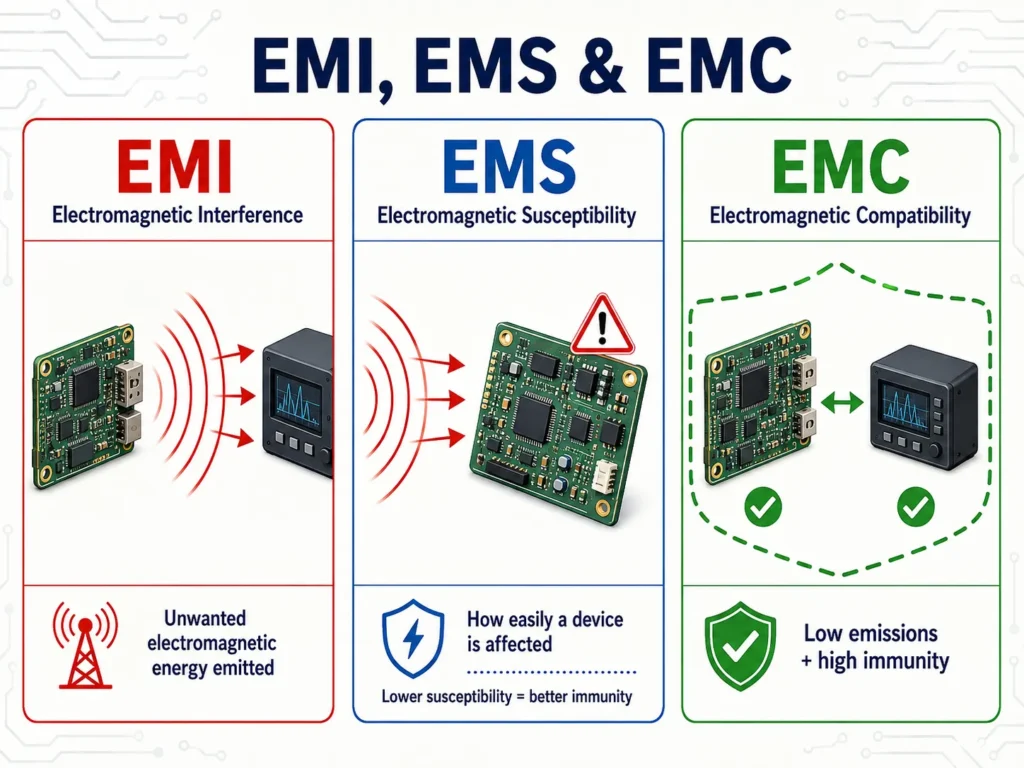
EMI is unwanted electromagnetic noise. EMS describes how easily a device is affected by that noise. EMC is the ability of products to operate without creating or suffering unacceptable interference.
This guide explains the EMI EMS EMC difference, its effect on PCB layout, and the main standards to review before testing.
What Is EMI?
EMI stands for electromagnetic interference. It is an unwanted electromagnetic disturbance that can reduce device performance. It may come from inside or outside the product.
Common internal sources include switching power supplies, high-speed clocks, digital data lines, motors, relays, and wireless transmitters. External sources include nearby radio equipment, power lines, electrostatic discharge, and other electronic products.
EMI normally reaches a circuit in one of two ways:
- Conducted EMI travels through power cables, signal wires, ground connections, or other conductive paths.
- Radiated EMI travels through the air as an electromagnetic field. PCB traces, cable loops, and openings in an enclosure can act as antennas.
Every EMI problem has three parts: a noise source, a coupling path, and a victim circuit. Engineers can improve the design by reducing the noise at its source, interrupting the coupling path, or making the victim less sensitive.
What Is EMS?
EMS stands for electromagnetic susceptibility. It describes how strongly a device responds to an electromagnetic disturbance. A highly susceptible circuit may reset, lose data, show measurement errors, or stop working when exposed to noise.
EMS is closely related to electromagnetic immunity. The two ideas point in opposite directions. High susceptibility means low immunity. High immunity means the device can continue to work correctly in a noisy environment.
Susceptibility problems often appear at high-impedance inputs, long traces, unprotected connectors, reset lines, analog sensor paths, and poorly referenced digital signals. Typical immunity tests expose the finished product to electrostatic discharge, radiated radio-frequency fields, electrical fast transients, surges, or conducted RF disturbances.
Pass criteria depend on the product and standard. A temporary change may be allowed in some tests, but safety-related equipment can have stricter limits.
What Is EMC?
EMC stands for electromagnetic compatibility. It is the overall ability of equipment to work correctly in its intended electromagnetic environment. The equipment must not create excessive disturbances. It must also tolerate the disturbances it is expected to encounter.
EMC therefore includes two sides:
- Emission control: Limit the conducted and radiated noise produced by the device.
- Immunity control: Keep the device operating correctly when external electromagnetic disturbances are present.
A product can have low emissions but poor immunity, or strong immunity while creating too much noise. A successful design must address both. This principle is reflected in the European Commission’s EMC Directive overview.
EMI vs EMS vs EMC: Key Differences
| Term | Main Meaning | Key Question | Typical Evaluation | PCB Design Goal |
|---|---|---|---|---|
| EMI | Unwanted electromagnetic disturbance | What noise does the product create or receive? | Conducted and radiated emission measurements | Reduce noise sources and coupling paths |
| EMS | Sensitivity to electromagnetic disturbance | How easily does noise disrupt the product? | ESD, RF field, surge, EFT, and conducted immunity tests | Protect sensitive circuits and improve immunity |
| EMC | Acceptable emissions plus adequate immunity | Can the product operate without causing or suffering unacceptable interference? | Applicable emission and immunity test program | Meet the complete system-level compatibility target |
In simple terms, EMI is the disturbance, EMS is the response to that disturbance, and EMC is the desired result. This relationship helps teams organize design reviews and test plans.
How PCB Design Affects EMC Compliance
EMC is a system property. Enclosures, cables, power supplies, firmware modes, and accessories all matter. Yet the PCB often controls the main noise loops and coupling paths.
Use a Clear Layer Stack-Up and Continuous Reference Planes
High-speed signals need a nearby and continuous return plane. A broken return path forces current to travel around a slot or gap. This increases loop area and radiation. It can also increase crosstalk and signal distortion.
Place critical signal layers next to solid ground planes when possible. Avoid routing high-speed traces across plane splits. Add ground stitching vias near layer changes when they support the return path. For fast or RF circuits, review the stack-up and impedance before layout. These steps are central to high frequency PCB design.
Control Trace Routing and Loop Area
Keep clocks, switch nodes, and other high-energy traces short. Route differential pairs together and maintain the intended impedance. Separate noisy switching areas from sensitive analog, RF, and sensor circuits.
Return current follows the path of lowest impedance. At high frequency, it tends to flow close to the signal trace on the reference plane. Vias, plane gaps, and poor connector pin assignments can disturb this path. Smaller loops usually radiate and receive less noise.
Place Decoupling Capacitors Close to Power Pins
A decoupling capacitor supplies short current bursts close to an IC. This reduces the high-frequency current loop. Use short, wide connections and a low-inductance path to the power and ground planes.
One capacitor value may not control the full noise range. Package size, mounting inductance, plane structure, and regulator behavior also matter. Evaluate the complete power distribution network.
Filter Noise at Power and I/O Boundaries
Connectors and cables can carry conducted noise and can become efficient antennas. Place filters and protection parts near the point where a signal or power line enters the board. Keep the unfiltered path short and separate it from the filtered side.
In an EMI filter PCB layout, placement is as important as the schematic. Long traces and shared return paths can bypass a filter. Select parts for the real frequency, current, voltage, and signal requirements.
Plan Shielding and Ground Connections as One System
PCB EMI shielding can help when source control and routing are not enough. Shield cans, conductive enclosures, gasket contacts, and cable shields need a low-impedance connection to the correct reference. A long grounding lead can make a shield ineffective at high frequency.
Shielding adds cost, weight, thermal issues, and assembly steps. Start with the source, coupling path, and victim model. Add shielding where measurements show a clear benefit.
Review Manufacturability Before Prototypes
Trace geometry, materials, via structures, and stack-up tolerances affect the finished board. An early DFM review aligns electrical targets with the manufacturing process. Review Benlida’s PCB manufacturing services before releasing production files.
Near-field probes, current probes, spectrum analysis, and bench immunity checks can reveal weak areas early. See Benlida’s PCB compliance testing information for board-level inspection options. Plan final regulatory testing for the complete product and its normal operating modes.
Key EMC Standards for Electronics
Requirements depend on the product, market, power source, radio functions, and environment. A multimedia standard may not apply to automotive, industrial, or medical equipment. Confirm the plan with a qualified laboratory before design release.
FCC Part 15 in the United States
47 CFR Part 15 contains rules for radio-frequency devices in the United States. It covers intentional, unintentional, and incidental radiators. Digital products without an intentional transmitter are commonly evaluated under Subpart B for unintentional radiators. FCC Part 15 mainly addresses emissions. It is not a general immunity standard.
CE Marking and the EU EMC Directive
CE marking is not one EMC test or one standard. It indicates that the manufacturer has assessed the product against all applicable EU legislation. Under Directive 2014/30/EU, equipment must limit electromagnetic emissions and provide adequate immunity for its intended use.
Manufacturers identify the applicable requirements, prepare technical documentation, issue an EU Declaration of Conformity, and affix the CE mark when the product conforms. Harmonised European standards can provide a presumption of conformity. Always review the European Commission’s current EMC harmonised standards list.
CISPR 22, CISPR 32, and CISPR 35
CISPR 22 was widely used for information technology equipment emissions. It is now a legacy standard. The IEC lists it as withdrawn and replaced by CISPR 32, which covers emission requirements for multimedia equipment.
For multimedia equipment immunity, engineers should also review CISPR 35. Other product groups use different standards. Examples include industrial, automotive, household, lighting, and medical equipment. Do not select a standard only because a similar product used it in the past.
Frequently Asked Questions
Are EMI, EMS, and EMC the same?
No. EMI is the disturbance. EMS is a device’s susceptibility to it. EMC means the equipment limits emissions and has enough immunity for its intended environment.
Is EMS the same as electromagnetic immunity?
They describe opposite sides of the same behavior. Higher susceptibility means lower immunity. Modern standards often use immunity when describing resistance to external disturbances.
Can a bare PCB receive EMC certification?
Usually, compliance applies to finished equipment, not an unpowered bare PCB. Enclosures, cables, software modes, power supplies, and accessories affect results. Good PCB design still reduces risk.
What are the most effective ways to reduce PCB EMI?
Use solid return paths, small loops, short high-speed traces, close decoupling, and connector filtering. Separate noisy and sensitive circuits. Measure early to find the actual source and coupling path.
Build EMC into the PCB from the Start
Understanding the EMI EMS EMC difference helps prevent problems before formal testing. A controlled stack-up, careful routing, and early measurements reduce redesign risk and improve reliability.
Benlida supports PCB manufacturability review, fabrication, and board-level quality control for prototypes and volume production. Get an EMC-ready PCB quote and discuss your stack-up, materials, impedance, and test needs with our team.