PCB Solder Resist: Types, Design Rules, and Best Practices
PCB solder resist, often called solder mask, is a permanent polymer coating over most of a circuit board’s copper. It helps reduce solder bridging during assembly. It also protects traces from oxidation, contamination, and handling damage. Pads and other selected areas remain open for soldering or electrical contact.
The main process categories are liquid photoimageable solder resist, dry-film photoimageable solder resist, and conventional non-photoimageable liquid solder resist. LPI is the common choice for many modern rigid PCBs. Still, the best option depends on feature size, board construction, color, surface finish, and the fabricator’s qualified process.
What Is PCB Solder Resist?
Solder resist covers copper that should not receive solder. It adds insulation and limits contact with exposed metal. The coating does not replace correct conductor spacing, conformal coating, or other environmental protection.
Solder resist and surface finish have different jobs. The mask protects most of the copper. The surface finish protects the pads and other copper that must remain exposed. Both processes must work together, but one does not replace the other.
The IPC solder mask handbook covers material selection, processing, defects, and final-finish interactions. IPC-SM-840 addresses permanent solder mask qualification and performance. It does not set every factory’s layout rules. The released fabrication drawing and supplier-approved rules still control the job.
Types of PCB Solder Resist
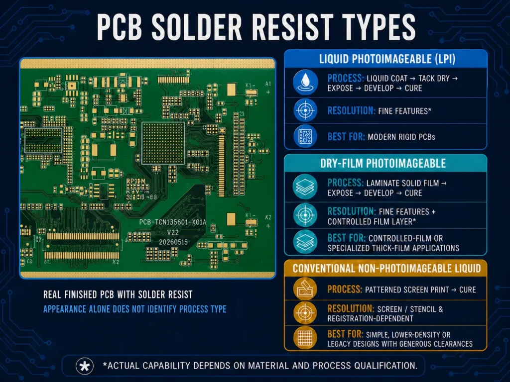
Terms such as “LPI,” “dry film,” and “ink” are often mixed together. LPI is itself a liquid ink. A clearer comparison separates liquid photoimageable materials, dry-film photoimageable materials, and traditional non-photoimageable liquid inks.
| Type | Process | Resolution | Cost | Best For |
|---|---|---|---|---|
| Liquid photoimageable (LPI) | Liquid coating, tack dry, image exposure, development, and final cure | Supports fine features when the material and process are qualified | Depends on coating route, imaging, volume, and yield | Most modern rigid PCBs and layouts with fine mask features |
| Dry-film photoimageable | Solid film lamination, image exposure, development, and cure | Supports fine features and a controlled film layer | Adds film storage, handling, and lamination | Applications that need a controlled film layer or a specialized thick-film process |
| Conventional non-photoimageable liquid solder resist | Patterned screen printing followed by cure | Depends strongly on screen or stencil and registration | Depends on screen preparation, volume, yield, and rework | Simple, lower-density, or legacy designs with generous clearances |
Actual resolution and cost also depend on board size, coating thickness, color, copper topography, volume, and factory equipment.
Liquid Photoimageable Solder Resist
LPI starts as a liquid applied by screen printing, curtain coating, or spraying. The board is tack dried, imaged, developed, and fully cured. Taiyo’s LPI product information shows that application, color, finish resistance, and feature capability vary by formulation.
Dry-Film Photoimageable Solder Resist
Dry film arrives as a solid sheet. It is laminated, exposed, developed, and cured. The film can provide a controlled layer and fine features. Eternal Materials lists dry-film solder masks for rigid, flexible, and substrate applications. The exact product must match the board construction.
Conventional Non-Photoimageable Liquid Solder Resist
This material is usually patterned by screen or stencil and then thermally or UV cured. It can suit simple boards with generous clearances. Pattern quality depends heavily on printing and registration. Confirm adhesion, thickness, cure, assembly temperature, and finish compatibility.
How to Set Solder Mask Dam and Opening Rules
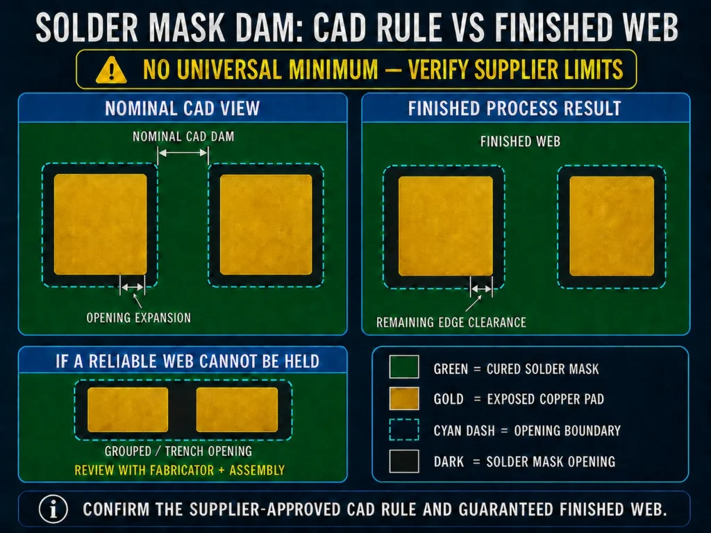
A solder mask dam, also called a web or sliver, is the strip of cured mask between two adjacent openings. A dam can help separate solderable areas. However, a very narrow dam may not image, develop, or remain attached reliably.
There is no universal minimum solder mask dam width. The finished limit depends on registration, imaging, copper topography, pad pitch, coating, formulation, color, and factory capability. Ask whether a quoted value is a nominal CAD rule or a guaranteed finished web.
Start With the Component Land Pattern
Follow the component manufacturer’s recommended land pattern first. A solder-mask-defined pad has an opening smaller than the copper pad. A non-solder-mask-defined pad has an opening larger than the copper pad. The right choice depends on the package, pad geometry, assembly process, and reliability goals.
Do not copy one package rule into every footprint. For example, Analog Devices application note AN-772 gives a 75 micrometer web example for one package. It is not a universal PCB fabrication limit.
Account for Registration and Process Tolerance
The CAD opening must allow for movement between the copper image and the mask image. If the expansion is too small, mask can encroach on a pad. If it is too large, the remaining dam can disappear. Review the worst-case result, not just the nominal CAD view.
When a reliable dam cannot remain between fine-pitch pads, the fabricator may recommend a grouped or trench opening. Review this with assembly needs because it removes the mask barrier between adjacent pads.
Define Via Treatment Separately
A via without a mask opening may be described as tented, but the result depends on via size, process, and board side. Tenting is not the same as plugging or filling. State whether vias must be open, tented, plugged, filled, or capped. Identify via-in-pad features separately.
Solder Resist Colors and Their Use Cases
Green is widely used and is usually easy to inspect because copper, pads, and markings remain visible. It also has broad material and process availability. This makes it a practical default, not a technical requirement.
Black can support a dark product appearance but may reduce inspection contrast. White is common in lighting products where reflectance matters. Blue, red, yellow, and other colors can support product identification or branding.
Color alone does not prove electrical reliability. Pigments can affect inspection, exposure, cure behavior, and optical performance. Available colors also vary by material. Confirm the formulation, gloss or matte finish, inspection method, and optical target before release.
Surface Finish Compatibility With Solder Resist
Common surface finishes include HASL, ENIG, immersion silver, immersion tin, and OSP. These finishes remain on exposed pads while the solder resist covers surrounding copper. Compatibility depends on the mask chemistry, surface preparation, cure profile, finish chemistry, and process sequence.
HASL adds heat and flux exposure. ENIG and other immersion finishes use chemical baths. OSP needs clean exposed copper and controlled handling. A supplier product page and its linked data sheets may list processing and finish resistance. That evidence applies only to the named material and process conditions.
Tell the fabricator the final finish. Identify gold fingers, contact areas, wire-bond pads, heat sinks, and other features that must stay free of mask.
Common Solder Resist Defects and Prevention
| Defect | Common Contributors | Prevention and Review |
|---|---|---|
| Misregistration or mask on a pad | Insufficient opening allowance, imaging alignment error, or panel movement | Use supplier-approved expansion rules and inspect pad-edge clearance |
| Peeling, lifting, or flaking | Contamination, weak surface preparation, incorrect cure, or incompatible processing | Control cleaning, surface condition, cure, and final-finish exposure |
| Pinholes or insufficient coverage | Air, debris, poor coating control, or difficult copper topography | Control coating and cleanliness, then inspect high-risk areas |
| Broken or missing mask dam | A web below process capability or excessive opening expansion | Widen the web, reduce the opening where allowed, or use a grouped opening |
| Cracking or discoloration | Incorrect cure, excessive thermal exposure, mechanical strain, or unsuitable material | Match the material and cure to the board construction and assembly profile |
Visual inspection should cover openings, registration, coverage, color, contamination, and surface damage. Acceptance criteria must match the purchase documentation and applicable requirements. Benlida’s PCB quality inspection page provides an overview of its publicly described quality-control process.
Solder Resist Data to Include in PCB Files
Clear fabrication data reduces assumptions and revision cycles. Include the following information when it applies:
- Top and bottom mask layers aligned with the copper data.
- Solder resist color and gloss or matte appearance.
- Surface finish and any areas that must remain free of mask.
- Package-specific mask-defined or non-mask-defined pads.
- Critical opening expansion, dam, or registration requirements.
- Via treatment and any via-in-pad features.
- Required material qualification, thickness, inspection, or acceptance criteria when contractually important.
Keep the fabrication drawing, Gerber or ODB++ data, drill files, and readme notes consistent. Flag rules tighter than the supplier’s stated capability. See Benlida’s PCB manufacturing services for its publicly described fabrication workflow.
PCB Solder Resist FAQ
What Is the Minimum Solder Mask Dam Width?
There is no single minimum for every PCB. It depends on material, imaging, registration, coating, color, and factory controls. Ask for a guaranteed finished value and its matching CAD rule. If a fine-pitch layout cannot hold a stable dam, review a grouped opening.
What Is the Difference Between LPI and Dry-Film Solder Resist?
LPI is coated as a liquid. Dry film is laminated as a solid sheet. Both can be photoimaged and developed. LPI is common on modern rigid PCBs. Dry film can provide a controlled layer for specialized applications. The product must match the board construction and process.
Does Solder Resist Color Affect PCB Performance?
Color alone does not set electrical performance. Pigment and formulation can affect imaging, cure, inspection contrast, reflectance, and thermal appearance. Confirm the selected material for the board process. Lighting and optical products may need a defined reflectance target.
What Causes Solder Mask Peeling Defects?
Contributors include contamination, poor precleaning, weak adhesion, incorrect exposure or development, improper cure, chemical incompatibility, and thermal or mechanical stress. Prevention needs a qualified material, controlled processing, and inspection against the released acceptance requirements.
Need Help Reviewing Solder Mask Requirements?
Share your Gerber or ODB++ files, solder mask requirements, surface finish, via treatment, and fine-pitch details with Benlida. The team can review the project requirements and prepare a PCB manufacturing quote.

