PCB Via Types: Through-Hole, Blind, Buried, and Microvia
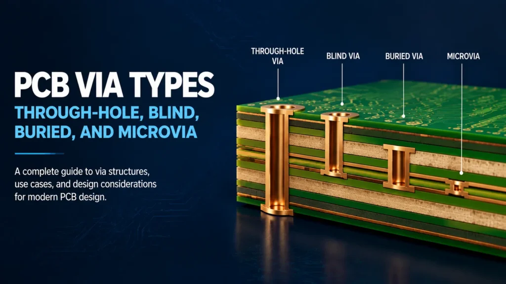
A PCB via is a conductive interconnect between copper layers. Through-hole via, blind via, buried via, and microvia are four common terms, but they are not defined on one axis. Through-hole, blind, and buried identify where a via starts and ends. Microvia describes a small structure, commonly formed by laser drilling. A microvia can also be blind or buried.
A plated through via is usually the simplest choice. Blind and buried vias preserve routing space outside their spans. Microvias support dense HDI routing. Extra drill, lamination, fill, and inspection steps can change cost and risk. Select the structure after the stack-up and package escape plan are clear.
What Is a PCB Via?
A PCB via carries signal, power, ground, or heat between copper layers. Most begin as drilled or ablated openings that are then metallized. A via is not automatically a component hole. A plated component hole accepts a lead, while a through via normally interconnects layers.
A through via barrel passes through the full board, but it does not electrically join every copper layer. It connects only to layers that have a pad tied to the barrel. Other layers use clearance openings, often called antipads.
This article focuses on conductive vias. Benlida’s broader guide to PCB hole types and applications also covers mounting holes, slots, press-fit holes, and other mechanical features.
IPC-6012F covers rigid boards with plated through holes, blind and buried vias, and microvias. Standards do not replace a fabricator’s qualified design rules. Purchase documents should identify the applicable specification, revision, performance class, and project requirements.
Through-Hole Vias
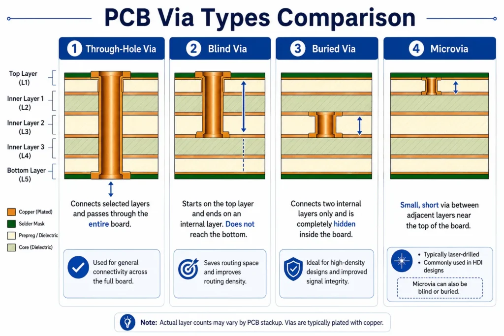
A through-hole via runs from one outer surface to the other. It is normally drilled after the multilayer stack is laminated. The hole is cleaned, metallized, and copper plated to create a conductive barrel. Pads connect the barrel to selected copper layers.
Through vias usually have the lowest starting process complexity. They work well for general multilayer routing, power and ground connections, test access, and thermal paths.
The tradeoff is routing space. The drill and clearance pattern can block every layer, even where no electrical connection is needed. The unused barrel can also form a signal stub. A Texas Instruments discussion of high-speed vias explains how the via barrel, pad, antipad, and stub affect signal behavior. High-speed designs may need backdrilling, a shorter span, or another verified structure.
Blind Vias
A blind via starts on one outer surface and ends on an internal layer. It does not pass through the full board. Depending on the geometry, it may be produced by controlled-depth mechanical drilling, laser drilling, or sequential lamination.
Blind vias help route dense packages because they leave deeper layers or the opposite surface available. They can shorten a connection and reduce the unused stub.
Cost is usually higher than for a basic through-via build. The fabricator may need extra drill files, depth control, lamination stages, plating controls, and inspection. The exact cost depends on the via span and manufacturing sequence. Freeze every start and stop layer before layout.
Buried Vias
A buried via connects internal layers and is not visible from either board surface. The fabricator drills and plates a core or sub-composite before it is laminated into the final board. Later lamination hides the structure inside the stack.
Buried vias preserve space on both outer surfaces and keep a connection within selected internal layers. This can help a dense layout, but geometry and return paths still control electrical behavior.
The process is more complex than a basic through-via build. It adds registration, plating, lamination, inspection, and yield considerations. A buried via can still be the better system choice if it avoids extra board area or layers. Review the complete construction with the selected multilayer PCB manufacturing process instead of comparing one hole price.
Microvias
A microvia is a small interconnect formed through a thin dielectric. Modern HDI microvias are usually laser drilled. A single microvia commonly connects adjacent layers. Successive lamination can create staggered or qualified stacked structures for longer routing paths.
Microvia is not simply another layer-span label. A surface microvia is also a blind via. A microvia formed in a sub-composite can become a buried structure after lamination. Not every blind via is a microvia because larger blind vias may be mechanically drilled.
Microvias support fine-pitch BGA escape and high routing density. They also bring extra process controls. Laser drilling, plating, filling, planarization, repeated lamination, and stacked interfaces can add cost. An IPC warning on microvia reliability discusses latent interface failures in some complex stacked, filled constructions. It does not mean every microvia will fail.
Use Benlida’s HDI PCB design rules for stack-up, aspect-ratio, land, and reliability planning. Then confirm the construction against the selected HDI PCB fabrication process. Published capability pages are a starting point, not project approval.
PCB Via Type Comparison
The table shows relative planning differences. It is not a universal price list. One board can combine several structures when the lamination sequence supports them.
Through-hole, blind, buried, and microvia comparison
| Via Category | Layer Relationship / Board Need | Typical Formation | Relative Complexity and Cost | Typical Use | Main Design Check |
|---|---|---|---|---|---|
| Through-hole via | Passes through the complete board; works on two-layer and multilayer boards | Usually mechanically drilled after full lamination, then plated | Usually the lowest starting complexity | General routing, power, ground, test, and thermal paths | Aspect ratio, annular ring, layer blockage, and high-speed stub |
| Blind via | Outer layer to selected inner layer or layers; requires a multilayer board | Controlled-depth mechanical drilling, laser drilling, or sequential processing | Usually higher than a basic through-via build | Dense package escape and shorter selected layer transitions | Exact start and stop layers, depth, registration, and plating |
| Buried via | Between internal layers; normally needs at least two internal copper layers | Drilled and plated in a sub-composite before final lamination | Higher due to sub-processing and lamination | Internal routing while preserving both outer surfaces | Buildable lamination order, registration, inspection, and yield |
| Microvia | Usually an adjacent-layer connection in an HDI build-up; may be blind or buried | Usually laser drilled, then plated; stacked designs may need filling and planarization | Process-dependent and often higher, especially with repeated lamination | Fine-pitch BGA escape and high-density routing | Dielectric depth, diameter, lands, fill, interfaces, and reliability plan |
How to Choose the Right Via Type
Start With the Required Layer Span
Use the simplest structure that reaches the required layers. A through via is often enough when layer blockage and stubs are acceptable. Choose a blind or buried span only when it solves a clear routing, package, or electrical constraint. Define the stack-up before assigning via rules.
Review Component Escape and Via-in-Pad
Fine-pitch BGAs may need small blind microvias or via-in-pad. Via-in-pad describes placement inside a component land, not a separate layer-span type. An open hole under a solderable pad can draw solder into the barrel or contribute to voiding. The package guideline and assembly process may require filling, planarization, and copper capping.
Check Electrical, Power, and Thermal Needs
For high-speed signals, review via length, stub, pad, antipad, reference-plane changes, and return vias. For power or heat, review copper area, barrel plating, current sharing, and the number and location of vias. More vias are not automatically better because holes and clearances also remove copper.
Count Manufacturing Steps, Not Just Via Count
Cost follows the process flow. Count drill programs, controlled depths, lamination cycles, laser steps, fill and cap operations, inspection, coupons, and reliability testing. Ask the fabricator to approve the full stack-up and drill matrix. A more expensive via can still reduce total cost if it avoids a larger board or extra layers.
Send separate, clearly named drill data for each via span. State whether dimensions are tool size, designed diameter, or finished hole size. Also identify filled, plugged, capped, tented, or open vias. The Würth Elektronik via-treatment guide shows why these terms are not interchangeable.
PCB Via FAQ
What Is the Difference Between a Blind Via and a Buried Via?
A blind via is accessible from one outer surface and ends on an internal layer. A buried via connects only internal layers and is hidden after final lamination. Both need a defined start layer, stop layer, drill method, and manufacturing sequence.
Why Do Microvias Cost More Than Through-Hole Vias?
Microvias often need laser drilling, thin build-up dielectrics, controlled plating, and sequential lamination. Stacked structures may also need filling, planarization, extra inspection, and reliability evidence. These steps often cost more than a basic mechanical through-via process. The actual difference depends on volume and construction.
Can Blind Vias and Buried Vias Be Used in the Same PCB?
Yes. A multilayer or HDI board can combine blind, buried, through, and microvia structures when the lamination sequence is buildable. The design team should freeze every span and review registration, plating, fill, test coupons, and reliability before routing is complete.
What Is Via-in-Pad and When Is It Used?
Via-in-pad places a via inside a component land. It is used for dense BGA escape, short electrical paths, or thermal transfer. Treatment depends on the package and assembly plan. For example, Analog Devices AN-617 calls for a filled, plated-flat via-in-pad in its WLCSP guidance to help prevent solder-joint voiding. This is package-specific guidance, not a universal dimension.
Discuss Your PCB Via Design
Share your Gerber or ODB++ files, stack-up, drill files, finished-hole requirements, via treatments, impedance targets, quantity, and reliability needs. Ask Benlida to review the construction and confirm the via options available for the project before the layout is released.

