SMT Process Defects — Causes and How to Prevent Them
SMT process defects can start during solder paste printing, component placement, or reflow. Common examples include uneven paste deposits, bridging, smearing, misplaced parts, wrong parts, and tombstoning. Prevention requires control across the full line. Stencil design, material condition, placement data, machine condition, and thermal profiling all matter.
A visible defect does not reveal a single, certain root cause. Teams should capture data at each stage and change one variable at a time. This approach protects SMT assembly quality and avoids moving a problem to the next process.

What Causes SMT Process Defects?
SMT defects often form through several connected factors. The board and stencil may be misaligned. Paste may release unevenly. A placement program may use the wrong revision. The oven may then turn an upstream variation into a solder defect.
Review design, materials, equipment, programs, and process data. Useful records include stencil files, paste lots, feeder setup, first-article results, SPI trends, placement records, AOI findings, and thermal profiles.
The table below provides a starting point. These are investigation paths, not automatic diagnoses.
| Observed Condition | Possible Contributors | First Evidence to Check |
|---|---|---|
| Insufficient paste | Blocked or damaged aperture, poor release, paste condition, weak board support | SPI volume trend, aperture condition, underside wipe, printer setup |
| Excess paste or print bridge | Large aperture, thick stencil, paste slump, alignment error, underside contamination | Deposit area and volume, stencil data, print alignment, paste handling |
| Smear or offset deposit | Stencil movement, poor gasketing, board warpage, support or separation problem | Deposit position, fiducials, board support, stencil underside |
| Shifted or rotated component | Coordinate error, fiducial problem, nozzle issue, board movement, paste offset | Program revision, placement image, nozzle record, board registration |
| Missing or wrong component | Feeder setup, reel mismatch, pickup failure, release failure, incorrect variant | BOM revision, feeder verification, pickup and release records, first article |
| Tombstoning after reflow | Unequal paste, pad or copper imbalance, placement skew, uneven heating | Paired deposit volumes, pad design, placement, temperatures at both ends |
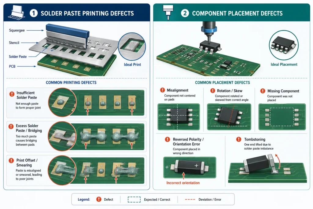
Solder Paste Printing Defects
SMT printing defects appear before components are placed. They should be measured at the printer whenever the process allows. Three-dimensional SPI can evaluate deposit height, area, volume, position, and bridging. Nordson lists these 3D solder paste inspection capabilities for its inspection platform.
SPI limits must match the approved assembly process. Each flagged deposit needs review. SPI does not prove finished-joint reliability or electrical function.
Insufficient solder paste
An insufficient deposit has less paste than the defined process window requires. It may increase the risk of opens, weak joints, or uneven wetting. It does not always create a failed connection.
Common contributors include blocked apertures, damaged stencil walls, poor paste release, and unstable paste condition. Board flex, weak support, or poor contact between the stencil and PCB can also reduce transfer.
Start with the location pattern. Repeated low volume at one aperture suggests a local stencil or design issue. Random low deposits require a wider review of paste condition, cleaning, support, and printer settings. Confirm storage, thawing, and stencil-life instructions with the paste supplier.
Excess paste and bridging
Excess paste increases the chance that nearby deposits will touch. Large apertures, an unsuitable stencil thickness, paste slump, or print misalignment may contribute.
A print bridge exists before reflow when adjacent deposits already connect. A solder bridge after reflow may have other causes. Placement offset, pad spacing, paste behavior, and the thermal profile may also contribute.
Compare SPI volume and area with approved limits. Inspect stencil data, alignment, board support, paste handling, and underside cleaning. Change apertures only after confirming a repeatable design issue.
Smearing and print offsets
Smearing means paste extends beyond its intended deposit boundary. It can increase bridging risk, but a small smear is not automatically an electrical short. Common causes include underside contamination, stencil movement, poor gasketing, warpage, and unstable board separation.
Use the defect map to see whether the shift is global or local. A global shift points toward registration, fiducials, or tooling. A local smear may point toward contamination, support, or a damaged area of the stencil.
Component Placement Defects
Placement begins with the correct released data. The BOM, centroid file, assembly drawing, polarity rules, feeder plan, and program revision must agree. A mechanically accurate machine can still place the wrong part if setup data is wrong.
Misalignment, rotation, and skew
A component placement error may come from wrong coordinates, poor fiducial recognition, board movement, or panel variation. Worn nozzles, weak vacuum, vision data, and machine drift can also contribute. Large paste offsets may change the component position before reflow.
Review the placement record and the board image before changing coordinates. Check whether the error follows one package, nozzle, head, feeder, panel position, or production lot. JUKI explains how laser centering can measure component position and angle. Available checks still depend on the machine model and configuration.
Missing, wrong, or reversed components
A missing part may result from an empty tape pocket, pickup failure, component loss, or incomplete release. A wrong part may come from a reel, feeder, splice, or variant mismatch. Reversed parts often point to orientation data, feeder loading, or polarity verification.
Use barcode or feeder verification where the approved process supports it. Recheck the reel during replenishment and splicing. Verify the first article against the released BOM and drawing. A size or marking check reduces risk, but it does not prove component authenticity.
Why tombstoning is not only a placement problem
Tombstoning appears when one end of a small passive rises during reflow. Off-center placement can increase the risk. So can unequal paste deposits, asymmetric pads, nearby copper, and uneven heating. Placement force and Z-height may also affect the starting condition.
Indium Corporation’s tombstoning guidance connects printing, placement, stencil design, and thermal balance. Surface tension may correct a small offset during wetting. It cannot reliably repair a severe print or placement error.
Reflow-Related Defects
Reflow melts the deposited solder and forms the joints. The profile must fit the solder paste, components, PCB materials, and the actual assembly’s thermal mass. A copied oven recipe is not proof that every location reached the required process window.
Printing or placement variation may become more visible after heating. Bridges, opens, tombstoning, poor wetting, or solder balls can therefore have upstream contributors. Oven changes cannot correct a wrong component, missing paste, or incorrect land pattern.
For a deeper thermal troubleshooting workflow, see the guide to reflow soldering defects. Review the measured profile together with paste, placement, pad design, and inspection data.
Stencil Design Rules to Prevent Printing Defects
Stencil thickness, aperture size, aperture shape, and area ratio affect paste release. IPC’s current revision table lists IPC-7525C, Stencil Design Guidelines. This guidance does not replace validation on the actual assembly.
- Start with the package and land pattern. Review pitch, pad size, thermal pads, bottom-terminated components, and required solder volume.
- Select thickness for the component mix. Fine features and large thermal pads may demand conflicting volumes. A stepped stencil may help, but it needs validation.
- Check aperture release. Calculate area and aspect ratios. Review wall quality, paste type, and supplier guidance before approving very small apertures.
- Use local aperture changes. Reductions, home-plate shapes, or segmented openings should address a defined risk. One rule will not fit every component.
- Validate with process data. Run a first article and review SPI distribution. Confirm that the design remains stable across boards, panels, and normal line pauses.
Set stencil-cleaning intervals from evidence. Product density, paste, aperture size, environment, and equipment all affect the right frequency. A fixed interval without SPI or defect trends may hide drift or waste production time.
Placement Machine Calibration and Quality Control
Calibration supports accuracy but cannot prevent every placement defect. Quality control must also cover released data, feeders, nozzles, vacuum, board support, vision, placement force, and Z-height.
Start each product with an approved program and verified material setup. Check fiducial recognition and panel orientation. Inspect critical parts on the first article. Record corrections instead of relying on an operator’s memory.
Monitor actual production results. Look for X-axis, Y-axis, and rotational error by component type and board position. Track repeatability and process capability under defined conditions. A machine specification is not the same as verified accuracy on every product.
Visible placement findings can be reviewed with AOI inspection. AOI coverage depends on optical access and the inspection program. It does not prove electrical function or reveal every hidden joint condition.
Recheck accuracy after maintenance, relocation, collision, or a negative process trend. Follow the equipment maker’s procedure. Use the resulting data to decide whether adjustment, calibration, tooling repair, or program correction is needed.
SMT Process Defects FAQ
What is the most common cause of SMT printing defects?
There is no single most common cause for every line. Poor aperture release, stencil contamination, alignment error, paste condition, and printer setup are frequent starting points. Use SPI trends and defect location to narrow the cause.
How does stencil design affect solder paste printing quality?
Stencil thickness and aperture geometry control potential paste volume and release. Poorly matched openings can produce low, high, or unstable deposits. The design should match the package, pads, paste, equipment, and validated process window.
What causes component misalignment during SMT placement?
Possible causes include incorrect coordinates, fiducial errors, PCB movement, nozzle problems, pickup offset, vision-data errors, and machine drift. Paste misregistration and board variation can also affect the final position.
How is SMT placement accuracy measured?
Placement accuracy compares the intended location with the measured component location. Teams analyze X-axis, Y-axis, and rotational error across repeated placements. They may also track repeatability and Cpk under defined test conditions. Product-level results should confirm machine specifications.
Discuss SMT Defect Controls Before Production
Define the process and inspection plan before releasing a PCBA build. Share the Gerber files, BOM, centroid data, assembly drawings, quantities, and critical-component notes. Identify any SPI, AOI, X-ray, electrical, or functional requirements that apply to the project.
Benlida’s SMT assembly services page provides an overview of the assembly flow.
and ask for a project-specific review of files, process controls, inspection scope, and quotation requirements.

