An assembled board can carry every component in the right place and still hide a manufacturing defect: a solder short between two pins, a resistor with the wrong value, a capacitor with reversed polarity. In-circuit testing finds these defects by checking each component individually while the board is unpowered, which is why it is the standard electrical test for high-volume PCB assembly.
This guide covers how in-circuit testing works, what it checks, the fixture and cost structure, how it compares with flying probe and functional testing, and when it is the right choice for your production volume.
Key takeaways — the decisions that matter for in-circuit testing:
- ICT is the highest-coverage electrical test for populated boards, catching up to 98 percent of component-level faults, with practical production coverage running between 85 and 90 percent because some nets are inaccessible to the fixture.
- The fixture is the economic gate: a bed-of-nails fixture costs on the order of twenty thousand dollars and takes weeks, so ICT only pays off at high volume, where the fixture cost spreads across thousands of boards.
- ICT verifies assembly correctness, not product behavior, so it complements rather than replaces functional test, which powers the board and catches design, firmware, and integration issues ICT cannot see.
- Testability is decided in layout: test points on a grid matching the fixture’s pin spacing determine coverage, and a board designed without them cannot be fully ICT-tested.
- ICT and flying probe are volume bookends, not competitors: flying probe handles prototypes and low volumes without a fixture, and ICT takes over as volume matures and the fixture amortizes.
What Is In-Circuit Testing (ICT)?
Definition
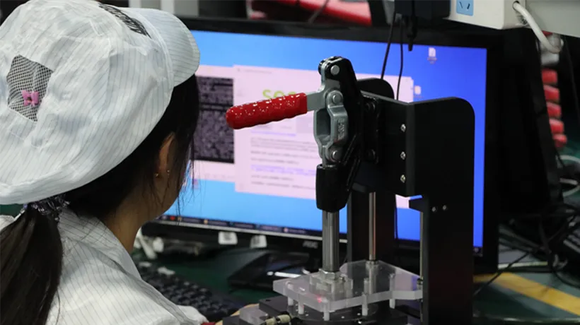
In-circuit testing (ICT) is an electrical test method that verifies each individual component on an assembled circuit board, without powering the board up. The method uses a bed-of-nails fixture, a custom-made array of spring-loaded probes that contact every test point at once, to measure components independently of the surrounding circuit. ICT is a white-box test: it knows the expected value of every component and compares each measurement against that value.
ICT is the fastest and most thorough electrical test for populated boards, which is why it dominates high-volume PCB assembly. A single ICT test can verify opens, shorts, resistance, capacitance, inductance, diode polarity, and component presence across the entire board in seconds. The method is cost-efficient for medium-to-high volume production because the per-board test cost drops once the fixture investment is spread across many boards.
Where ICT fits in the test flow
ICT belongs at the assembly stage, after soldering and before functional test. It catches manufacturing defects that AOI cannot see electrically and that functional test is not designed to isolate. The PCB testing guide positions ICT within the full test flow: AOI checks visible solder, ICT verifies electrical integrity at the component level, and functional test confirms the board performs its designed function.
Because ICT checks the structure of the assembly, it finds problems such as open connections, solder shorts, and missing or wrong components. Functional test, by contrast, verifies the product works as intended. The two methods answer different questions and are complementary, which is why high-volume lines run both.
From MDA to full in-circuit test
In-circuit testing evolved from manufacturing defect analysis (MDA), an earlier method that checked only for gross defects such as opens, shorts, and missing components. Modern ICT goes further: it measures component values, verifies polarity, programs devices, and checks analog and digital circuitry against the design. This depth is why ICT is the standard electrical test for high-volume PCB assembly rather than a simple pass-fail screen.
The evolution reflects the cost of escapes. A defect that passes a basic MDA screen can still cause a field failure, and in-circuit testing closes that gap by verifying each component to its specified value. For boards with complex analog circuitry, ICT is the only production test that isolates component-level faults reliably, which is why it remains the benchmark for dense, high-value assemblies.
How ICT Works
The bed-of-nails fixture
The heart of an in-circuit tester is the bed-of-nails fixture. The fixture holds a precise array of spring-loaded probes, or pogo pins, arranged to match the test points on the board under test. When the board is pressed down onto the bed, every probe makes contact with its corresponding test point simultaneously, connecting the tester to every net at once.
The fixture is custom-built for one board design, which gives ICT both its speed and its cost. Because all points contact at once, the tester can measure every component without moving a probe, finishing a full board test in seconds. That speed is the reason ICT suits high-volume production, but the custom fixture is also the reason it needs a mature, low-revision design to pay for itself.
The tester hardware and software
The in-circuit tester itself contains the measurement hardware: drivers and sensors that apply signals and measure responses at each probe. The software controls the test sequence, defines pass-fail limits for every measurement, and reports which components failed and where they are located. Modern in-circuit testers can also program microcontrollers, PLDs, and flash devices during the test, combining device programming with electrical verification.
An in-circuit tester measures components in isolation by using the probes to bypass the surrounding circuitry. This isolation is what makes ICT accurate: it verifies a resistor’s value without the parallel paths that would distort a normal in-circuit measurement. The result is component-level accuracy that no functional test can provide.
The test sequence
The test program runs a defined sequence on each board. It begins with opens and shorts verification across every net, then moves to component measurements: resistance, capacitance, inductance, and diode polarity. For boards with programmable devices, the sequence adds device programming and verification. Any failure is flagged with the component and its location, so rework targets the exact fault.
The sequence is built from the board’s netlist, which defines every net and the components and pins attached to it. A clean netlist is essential, because the test program verifies each measurement against it. Providing ODB++ or a complete netlist at the start of the project is what lets the test program be accurate on the first build rather than after debugging cycles.
The speed and accuracy of an in-circuit tester depend on the measurement hardware and the fixture quality. High-pin-count testers verify dense boards in a single pass, while fixtures with reliable probe contact keep false failures low. Keeping the tester calibrated and the fixtures maintained is what sustains ICT yield at volume, and it is the reason ICT programs budget for regular calibration alongside production testing.
What ICT Tests & Coverage
Defects ICT detects
In-circuit testing verifies the electrical integrity of every component and connection. The primary checks are opens, shorts, and continuity: it confirms every net is connected and that no two nets are shorted together. Beyond connectivity, ICT measures component values, checking resistance, capacitance, inductance, and diode polarity against the design’s expected values, which catches missing parts, wrong-value parts, and reversed polarity.
ICT also verifies that components are present and correctly oriented. A capacitor placed with reversed polarity, a resistor swapped for the wrong value, or a missing IC are all caught by the test. Because the measurements are component-level and repeatable, ICT finds these defects without human error and flags each one with its location for fast rework.
Coverage and its honest limits
In-circuit testing is the highest-coverage electrical method for populated boards, capable of catching up to 98 percent of component-level faults. In practice, the coverage achieved on a production board runs between 85 and 90 percent, because a small fraction of nets are physically inaccessible to the fixture. Those inaccessible nodes require boundary scan or a complementary test method to cover.
ICT has other honest limits. It cannot verify that a board functions as a product, only that it was assembled correctly. It cannot test connectors reliably, because the fixture probes internal test points rather than external interfaces. And it requires test points on every net to be verified, which is why boards designed for ICT carry a deliberate test-point pattern. Acceptance of the assembled board follows the IPC-A-610J standard, while qualification and performance requirements for the rigid bare board follow IPC-6012F.
Defects ICT catches in practice
In production, ICT catches a consistent set of faults. The most common are solder shorts between adjacent pins, which AOI can miss when the bridge is subtle, and open connections from insufficient solder or poor wetting. ICT also catches wrong-value components, reversed electrolytic capacitors and diodes, and missing parts that a visual inspection can overlook at speed.
Because ICT reports the exact component and net for every failure, it turns rework from a search into a targeted action. A technician goes straight to the flagged part instead of probing the board manually. This diagnostic precision is a large part of ICT’s value in high-volume production, where every minute of rework time multiplies across thousands of boards.
ICT Fixtures & Cost
The bed-of-nails fixture investment
The defining cost of in-circuit testing is the fixture. A bed-of-nails fixture is custom-designed and manufactured for one board, and it costs on the order of twenty thousand dollars, with complex boards pushing that higher. The fixture also takes weeks to build, because every probe position must match the board’s test-point layout precisely.
That fixture is the reason ICT is a volume decision. A fixture costing tens of thousands of dollars only makes economic sense when it is used across thousands of boards. For a prototype or a low-volume run, the fixture cost per board is prohibitive, which is why fixtureless methods such as flying probe testing take over at low volume.
Cost structure and break-even
ICT has a high fixed cost and a low variable cost. The fixture is the fixed cost, paid once. The per-board test cost is low, because a test takes only seconds and the fixture amortizes across every board. The break-even point against flying probe testing sits where the fixture investment is offset by faster per-board testing at high volume.
Below that volume, flying probe wins on total cost. Above it, ICT wins. The exact crossover depends on board complexity, test cycle time, and the number of design revisions expected. For boards with frequent revisions, ICT is a poor fit, because each revision can require a fixture change or rebuild, erasing the volume savings.
Fixture types and maintenance
Bed-of-nails fixtures come in several forms, from simple vacuum-actuated fixtures for double-sided boards to motorized and pneumatically driven fixtures for complex assemblies. Vacuum fixtures are common for single-sided and moderate boards; motorized fixtures add speed and accuracy for high-density layouts where probe alignment is critical.
Fixtures need regular maintenance to stay reliable. Probes wear with repeated contact, boards flex the fixture, and debris can interfere with contact, all of which produce false failures over time. A maintenance schedule that checks probe condition, verifies alignment, and recalibrates the fixture keeps ICT yields stable and prevents the expensive mistake of reworking boards that actually passed.
ICT vs Flying Probe
In-circuit testing and flying probe testing both verify assembled boards electrically, but they sit at opposite ends of the speed-versus-fixture-cost trade-off. ICT contacts every point at once through a fixture; flying probe moves probes to each point serially. The table compares them.
| Dimension | ICT | Flying probe |
|---|---|---|
| Fixture | Custom bed of nails, ~$20,000 | None |
| Test speed | Seconds (all points at once) | Slower (serial probing) |
| Coverage | Up to 98%, typically 85-90% | High, approaches ICT with advanced features |
| Best volume | High volume | Prototype to medium |
| Design changes | Fixture rebuild | Program update |
ICT delivers the highest coverage and speed of any electrical test method, which is why it is the benchmark for high-volume production. Flying probe offers fixtureless flexibility and adapts to design changes in a programming update, which suits prototypes and low volumes. The ICT vs flying probe comparison quantifies the trade-off in full detail.
Many production lines run both: flying probe for prototypes and new designs, then ICT once a design matures to high volume. The two methods also complement each other on a single line, where flying probe covers first articles and ICT covers steady-state production.
In practice, the crossover between the two is a volume and revision decision. A design expected to stay stable for a year at high volume justifies the ICT fixture. A design still changing weekly does not, because each revision may require fixture rework. Many contract manufacturers keep both capabilities and move boards between them as the product lifecycle dictates, which is why the choice is rarely one method over the other but rather which method at which stage.
ICT vs Functional Test
In-circuit testing and functional testing answer different questions. ICT verifies that the board was assembled correctly, checking each component in isolation while the board is unpowered. Functional testing powers the board and verifies that it performs its designed function. A board can pass ICT and still fail functional test if the firmware is wrong or two subsystems do not communicate.
ICT isolates faults to the component level, which makes rework fast and targeted. Functional test gives a pass-or-fail verdict on the whole product but does not pinpoint which component caused a failure. The two methods are complementary: ICT catches manufacturing defects early and cheaply, while functional test catches design, firmware, and integration issues that only appear under real operating conditions.
In practice, high-volume lines run ICT for manufacturing verification and functional test as the final product gate. A board that passes both is verified at the component level and at the system level, giving the highest confidence before shipment. For boards that need firmware programming, the functional test often performs the programming as part of the test sequence. The PCBA functional testing guide covers functional test development in depth.
Industries that run both ICT and functional test include automotive electronics, medical devices, industrial automation, and telecommunications, where a board that passes ICT can still fail on a firmware path or an interface timing requirement that only appears under real operating conditions. The two tests together cover the gap between correct assembly and correct function, which is why quality programs treat them as a pair rather than alternatives.
Test Points for ICT
What ICT needs from test points
In-circuit testing depends on test points that align with the bed-of-nails fixture. Every net that must be verified needs an accessible test point, and those points must sit on a grid that matches the fixture’s probe spacing. A board designed without a proper test-point pattern cannot achieve full ICT coverage, because the fixture has nowhere to land.
ICT test points differ from flying probe points. The bed of nails requires a regular grid, because the fixture’s probes are fixed at defined spacings, whereas flying probe can reach points at any location. ICT test points also need a minimum pad size that the spring-loaded probe can contact reliably, and clearance so adjacent probes do not interfere.
Design rules for ICT testability
Design for testability for ICT starts in layout. Place test points on both sides of the board where needed, keep them clear of components taller than the probe travel, and use a pad size and finish that withstand repeated probing. Dedicated test points are always better than relying on component pads, which risk damage and produce unreliable contact.
Boards intended for ICT should be designed knowing the fixture’s pin spacing, and the test-point layout should be documented for the fixture builder. Getting this right during design avoids the expensive outcome of a board that is electrically sound but physically impossible to test. The PCB test points design guide covers sizes, spacing, and the full set of placement rules.
Common test-point mistakes
The most common design mistake is relying on component pads and vias instead of dedicated test points, which limits coverage and risks probe damage to the components. Another is placing test points under tall components or on the wrong side of the board, where the fixture cannot reach them. A third is designing the layout without knowing the fixture’s grid, forcing a non-standard fixture that costs more.
These mistakes surface at the fixture-build stage, where they are expensive to correct. Catching them during design review is nearly free. A simple rule prevents most of them: place a dedicated, reachable test point on every net that must be verified, sized and spaced for the fixture, and confirm the layout against the fixture builder’s requirements before release.
When to Use ICT
In-circuit testing pays off when the volume is high enough to amortize the fixture and the design is stable enough that the fixture does not need constant rework. The scenarios below are where ICT delivers the most value.
- High-volume production. When thousands of boards must be tested, ICT’s speed and low per-board cost make it the most economical electrical test.
- Mature products. A design with few expected revisions suits ICT, because the fixture investment is not wasted on constant rework.
- Complex assemblies. Boards with many components and dense circuitry benefit most from ICT’s component-level accuracy.
- Visible test points. Boards designed with a proper test-point grid can achieve high ICT coverage.
- Repetitive quality demands. When every board must be verified to a consistent standard, ICT removes human error from electrical testing.
ICT is a poor fit for prototypes, low volumes, and designs still in rapid revision, where flying probe is the better choice. It also cannot replace functional test, which verifies product behavior. The decision framework for choosing test methods is covered in the PCB testing guide.
When planning ICT, confirm the manufacturing partner has the capability and the fixture experience for your board type. A partner that runs ICT in-house can build the fixture, generate the test program from your netlist, and iterate quickly if the program needs debugging. Discussing test strategy before the design locks is the difference between a test plan that runs smoothly and one that stalls at fixture build.
ICT Testing Checklist
Use this checklist to prepare a board for in-circuit testing and confirm coverage before committing to production.
- Test points placed on every net that needs verification, on the correct grid
- Test point pad size and spacing match the fixture probe requirements
- Test points clear of tall components that block probe travel
- Fixture designed and built to the board’s test-point layout
- Test program reviewed against the netlist on first build
- Coverage confirmed, including inaccessible nets flagged for boundary scan
- Pass-fail limits defined for RLC, polarity, and continuity measurements
Related reading
Dive deeper into the test methods covered in this guide:
- PCB testing guide
- Flying probe testing
- ICT vs flying probe
- PCB test points design
- PCBA functional testing
- PCB testing services
FAQ
What is in-circuit testing (ICT)?
In-circuit testing is an electrical test method that verifies each component on an assembled circuit board individually, without powering the board. It uses a bed-of-nails fixture to contact every test point at once and measures opens, shorts, resistance, capacitance, inductance, and polarity against the design’s expected values.
What does an ICT test check?
ICT checks the electrical integrity of every component and connection. It detects open circuits, solder shorts, incorrect resistance and capacitance values, reversed diode polarity, and missing or wrong components. It is a manufacturing gate that verifies the board was assembled correctly.
What is the difference between ICT and functional test?
ICT verifies that the board was assembled correctly by checking components in isolation while unpowered. Functional test powers the board and verifies it performs its designed function. ICT catches manufacturing defects; functional test catches design, firmware, and integration issues. High-volume lines run both.
How much does an ICT fixture cost?
A bed-of-nails fixture costs on the order of twenty thousand dollars, with complex boards costing more. The fixture is custom-built for one board design and takes weeks to produce, which is why ICT only pays off at high volume where the fixture cost spreads across many boards.
What is the difference between ICT and flying probe?
ICT contacts every test point at once through a custom fixture, making it fast but fixture-dependent. Flying probe moves probes to each point serially with no fixture, making it slower but flexible. ICT suits high volume; flying probe suits prototypes and low volume.
How much coverage does ICT provide?
ICT can catch up to 98 percent of component-level faults, with practical production coverage running between 85 and 90 percent. A small fraction of nets are inaccessible to the fixture and require boundary scan or a complementary test to cover.
Can ICT be used on prototypes?
Not economically. ICT requires a custom fixture costing tens of thousands of dollars, which is unjustifiable for a prototype or low-volume run. Fixtureless methods such as flying probe testing are the right choice at low volume.

