PCB Functional Testing Methods — FCT, ICT, AOI, Flying Probe & Boundary Scan
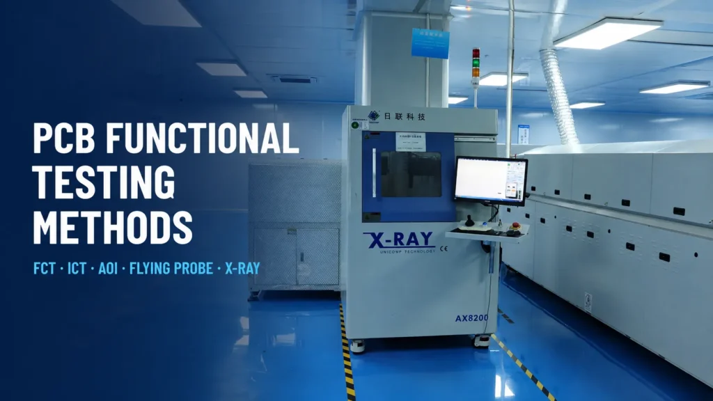
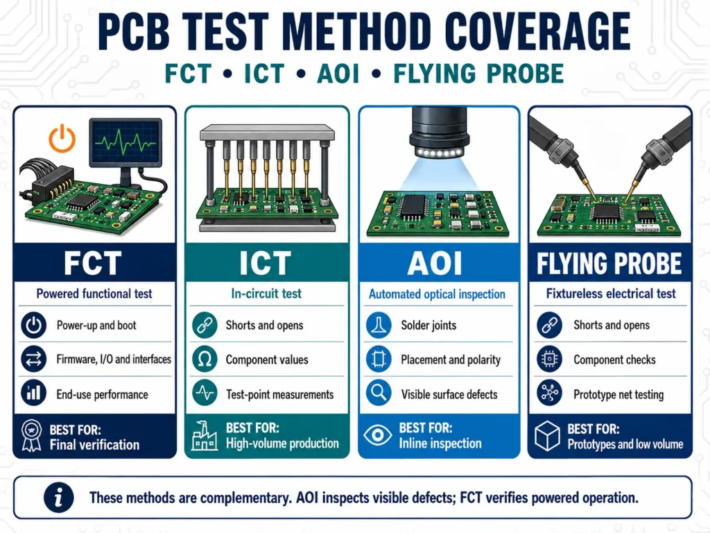
PCB assembly testing is not one single process. AOI checks visible workmanship. ICT and flying probe test electrical nodes and components. X-ray reveals hidden solder joints. Boundary scan checks supported digital interconnects. FCT powers the board and checks whether it works as intended.
These methods find different defects. A test plan that relies on only one method can leave important gaps. This guide explains the main PCB testing methods, their limits, and the information a buyer should provide when ordering a tested PCBA.
Why PCB Functional Testing Matters
A defect found during production is usually easier to diagnose and repair. A defect found after shipment can cause a return, field service, replacement freight, and a delayed product launch. It may also affect customer trust.
Testing should therefore match the board’s risk, design, and order volume. A simple consumer board may need AOI plus a basic function check. A control board with BGAs may also need X-ray. A stable, high-volume design may justify an ICT fixture. Safety-related or high-reliability products may need tighter limits, more records, and wider coverage.
No method proves everything. Good PCB quality control combines suitable checks at different production stages.
| Method | Main purpose | Best fit | Main limitation |
|---|---|---|---|
| AOI | Checks visible placement and solder defects | Fast in-line inspection | Cannot prove electrical function or see hidden joints |
| ICT | Checks nets and component-level electrical values | Stable, higher-volume production | Needs test access and a dedicated fixture |
| FCT | Checks powered operation, interfaces, and outputs | Final behavior verification | Needs a defined procedure, limits, and often a fixture |
| Flying probe | Checks nets without a bed-of-nails fixture | Prototypes and low-volume builds | Slower per board than ICT |
| X-ray | Inspects hidden solder joints and internal features | BGA, QFN, and other hidden joints | Does not prove circuit behavior |
| Boundary scan | Tests supported digital interconnects through JTAG | Dense boards with limited probe access | Requires compatible devices and design support |
How the Methods Work Together
A typical test flow starts with AOI after soldering. X-ray may then check BGAs, QFNs, or other hidden joints. ICT or flying probe can screen electrical nets and component values. Programming and FCT follow when the board must run approved firmware. Each stage removes a different type of risk. The exact sequence depends on the product, production volume, test access, and failure cost. It should be agreed before the first production build.
AOI — Automated Optical Inspection
Automated optical inspection uses cameras, lighting, and software to compare an assembled board with programmed criteria. AOI PCB inspection can find missing parts, incorrect orientation, placement shifts, lifted leads, solder bridges, and other visible defects. It is fast and works well as an in-line process check.
AOI cannot confirm that a board performs its intended function. It also cannot fully inspect solder joints hidden under packages such as BGAs and QFNs. As Nordson explains in its AOI guidance, hidden joints require another inspection method. AOI is valuable, but it should not replace electrical or functional tests.
ICT — In-Circuit Testing
ICT PCB testing uses probes to contact designed test points. A bed-of-nails fixture can access many points at the same time. The tester can check opens, shorts, resistance, capacitance, and other electrical conditions. It may also identify missing parts, wrong values, or polarity errors when the test program supports those checks.
ICT is fast and repeatable after the fixture and program are ready. This makes it useful for stable, medium- or high-volume products. However, the fixture adds non-recurring engineering cost. Design changes can also require fixture changes.
Test access must be considered during PCB design. Dense layouts with too few test pads reduce coverage. Keysight’s ICT overview also describes the role of board-specific bed-of-nails fixtures. Buyers should ask for the planned coverage before approving fixture cost.
FCT — Functional Circuit Testing
FCT powers the PCBA and simulates its operating conditions. The test may apply input signals, communicate through interfaces, switch loads, read sensors, or measure outputs. It answers the practical question: does this assembled board perform the required functions?
A useful FCT procedure needs clear input ranges, output limits, test steps, firmware requirements, connector definitions, and pass/fail rules. A fixture may be needed for safe and repeatable connections. A golden sample can help during development, but written limits are still important.
FCT can find system-level problems that AOI or ICT may miss. Examples include communication failures, incorrect firmware, timing problems, and outputs that fall outside their limits. However, FCT may only show that a function failed. It may not identify the exact component that caused the failure. Learn more about Benlida’s PCB functional testing service.
Flying Probe Testing
A flying probe tester moves several probes between test points under software control. It does not need a board-specific bed-of-nails fixture. Setup cost is therefore lower, and program changes are easier.
Flying probe testing is a practical choice for prototypes, engineering validation, and low-volume production. It can check opens, shorts, and selected component values. The trade-off is cycle time. Probes move point by point, so the method is usually slower than ICT for large production runs.
X-Ray Inspection for BGAs and Hidden Joints
X-ray inspection looks through packages and board materials. It is useful when solder joints are not visible to a camera. Common targets include BGA, QFN, bottom-terminated components, and some through-hole connections.
Depending on the equipment and inspection program, X-ray can reveal bridges, insufficient solder, voiding, lifted joints, and head-in-pillow defects. Nordson’s X-ray application guide lists these defects for hidden BGA and QFN joints. X-ray is an inspection method. It does not confirm firmware, communication, or complete board operation.
Boundary Scan Testing for JTAG-Enabled Designs
Boundary scan uses test logic built into compatible integrated circuits. The tester communicates through a JTAG test access port. It can control and observe supported device pins, check digital interconnects, and help program devices without a physical probe on every net.
This method is useful on dense boards where direct test access is limited. It can complement ICT and FCT. It does not cover every analog circuit or every device. Coverage depends on the components, JTAG chain, schematic, and test software. JTAG Technologies’ boundary-scan overview explains how the method uses embedded test logic for assembly testing, programming, and debug.
How to Specify Testing in Your PCBA Order
Do not write only “100% tested” on a purchase order. The phrase does not define the method, test coverage, limits, or records. Give the manufacturer enough information to build a repeatable plan.
- Define the required methods. State whether you need AOI, flying probe, ICT, X-ray, boundary scan, FCT, or a combination.
- Provide complete design data. Include Gerber files, BOM, centroid data, schematics, netlists, assembly drawings, and test-point information when available.
- Describe real operating conditions. List supply voltages, current limits, loads, inputs, outputs, interfaces, and test sequence.
- Set measurable pass/fail limits. Avoid instructions such as “output should be normal.” Give an acceptable range and measurement conditions.
- Control firmware and programming. Identify the approved firmware version, programming interface, configuration data, and verification method.
- Agree on fixture details. Confirm fixture cost, ownership, expected life, maintenance, storage, and changes after a PCB revision.
- Define records and traceability. State whether you need serial-number results, measurement logs, failure codes, yield reports, or a test coverage report.
- Set the failure process. Explain whether failed boards should be diagnosed, repaired, retested, quarantined, or reported before action.
Share these requirements early with your turnkey PCB assembly supplier. Early review can improve test access and prevent late fixture or schedule changes.
Frequently Asked Questions About PCB Functional Testing
What is PCB functional testing?
PCB functional testing powers an assembled board and checks whether it performs its intended functions. It may test interfaces, outputs, sensors, loads, communication, and firmware under defined conditions.
Is AOI the same as FCT?
No. AOI checks visible placement and solder workmanship. FCT checks powered behavior. A board can look correct in AOI and still fail FCT because of an electrical, firmware, or system-level problem.
What is the difference between ICT and flying probe testing?
ICT normally uses a dedicated bed-of-nails fixture and contacts many test points at once. It is fast for stable, higher-volume builds. Flying probe uses moving probes and needs no dedicated fixture, so it is often better for prototypes and lower volumes.
What should I provide for an accurate PCBA testing quotation?
Provide design files, schematics, test requirements, operating conditions, pass/fail limits, firmware, expected order volume, and required records. Also identify critical components and hidden joints that may need X-ray or another special inspection.
Build a Practical Test Plan for Your PCBA
The right test plan depends on board design, risk, volume, and required traceability. Send Benlida your PCB files, BOM, quantity, and test requirements. We can review the project and discuss a suitable combination of inspection, electrical testing, and FCT.

