

PCB Reverse Engineering — Process, Uses and Legal Considerations
What Is PCB Reverse Engineering?
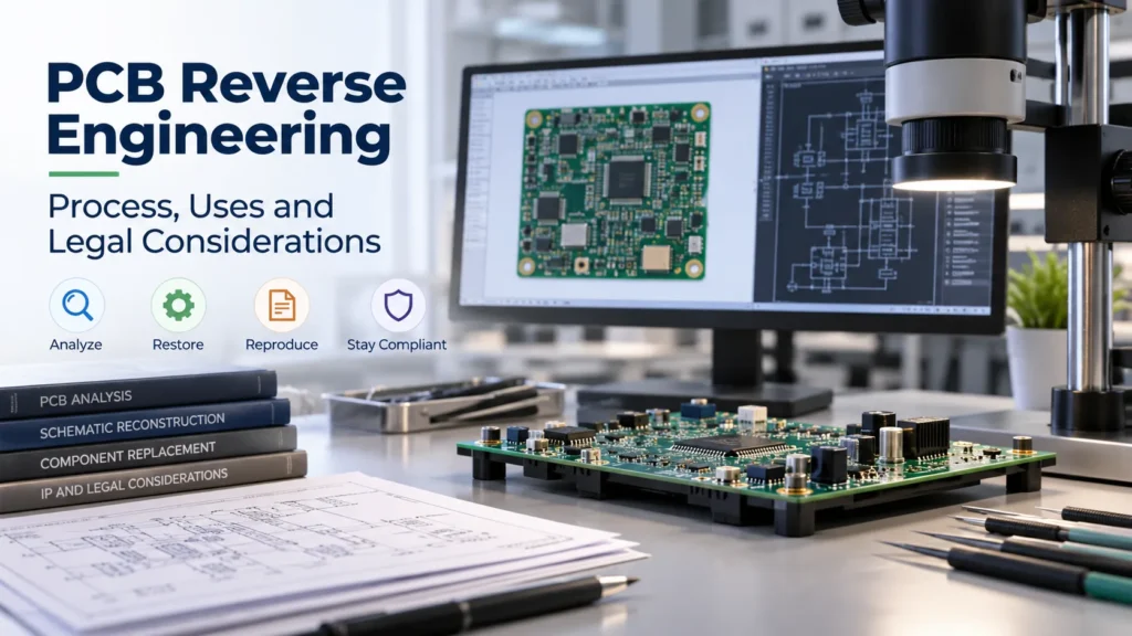
PCB reverse engineering analyzes an existing circuit board to reconstruct missing design information. The output may include a schematic, PCB layout, and bill of materials, or BOM. Common goals include legacy board replacement, obsolete part redesign, and documentation recovery.
It is not simply copying a photograph. Engineers must establish connections, identify components, and verify the reconstructed design. A bare PCB has no installed components. A PCBA includes them and may also depend on firmware that board tracing cannot recover.
Technical feasibility and legal permission are separate questions. Possessing a board does not automatically grant the right to reproduce its design or software. Before starting, define the intended use and check the applicable rights, permissions, and restrictions.
The Reverse Engineering Process — Scanning, Tracing, Schematic Recreation
A practical PCB reverse engineering process moves from evidence collection to a tested design. Agree on the authorized scope before any physical work, especially if the only sample may be damaged during inspection.
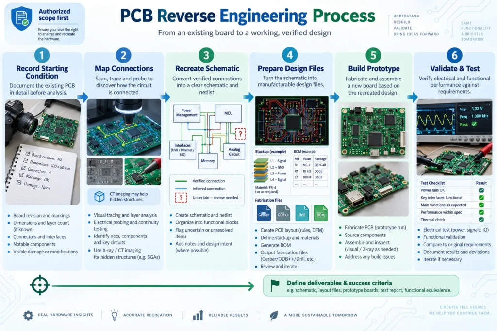
- Record the starting condition. Identify the board revision, dimensions, connectors, visible markings, modifications, and damage. Photograph both sides and compare available samples. A faulty board can contain broken traces or previous repairs that should not become design features.
- Map connections. Use suitable imaging and electrical measurements to establish which points connect. Surface scans do not reveal every inner-layer trace. Nikon’s guidance on CT imaging explains limitations involving flat parts and dense features. CT may help investigate hidden structures, but it does not guarantee complete design recovery. Any destructive layer inspection needs advance approval.
- Recreate the schematic. Convert verified connections into a netlist, which is a connection list, and organize them into circuit functions. The schematic describes electrical relationships; the PCB layout describes physical placement and routing. Mark uncertain connections and component identities for review.
- Prepare the design files. Confirm the layer stackup, materials, copper requirements, and mechanical constraints instead of guessing them from appearance. Build the layout and BOM around verified findings. Separate confirmed information from assumptions that still need measurement or engineering approval.
- Build and validate a prototype. Check the reconstructed files before manufacturing. Compare operation against agreed requirements and, where available, a known-good reference. A bare-board electrical test checks connections; it does not establish that an assembled board performs correctly.
Agree on the deliverables upfront. They may include editable CAD files, schematics, Gerber or ODB++ data, drill files, fabrication drawings, and a BOM. Assembled boards also need placement data, assembly instructions, and defined test or programming requirements.
Define what a successful replacement must do before the prototype arrives. List supply conditions, inputs, outputs, interfaces, loads, and pass/fail limits. Include calibration data and firmware versions where relevant. A board that powers on may still fail under load or communicate incorrectly. Record findings against a controlled hardware revision, and resolve open issues before releasing a production batch.
For a project discussion, review Benlida’s PCB reverse engineering services and ask which recovery methods and deliverables fit your board.
Common Legitimate Use Cases
Reverse engineering can support equipment maintenance and documentation recovery when the project has a valid legal basis. The business purpose alone does not settle that question. This table is an initial screening guide, not a legal determination.
Reverse Engineering Use Case
| Use Case | Legitimate? | Typical Deliverable |
|---|---|---|
| Recover missing company design files | Potentially, after confirming the company's rights and third-party restrictions | Reconstructed schematic, layout, and BOM |
| Replace a legacy equipment board | Potentially, with a lawful basis for analysis and the planned replacement | Replacement design and validation records |
| Replace obsolete components | Potentially, subject to design, software, and license rights | Revised BOM, affected design files, and test results |
| Assess third-party equipment compatibility | Jurisdiction- and method-dependent; review before work | Interface documentation and a compatibility assessment |
| Clone a third-party board for resale | Do not proceed without confirming the required legal basis | Scope and rights review before technical deliverables |
For example, a manufacturer may have a functioning machine but no replacement controller files. Reconstructing the controller could support continued maintenance. The team still needs to establish rights, firmware availability, and a suitable acceptance test. This is an illustrative scenario, not a Benlida customer case.
Legal Considerations Before Requesting Reverse Engineering
Is PCB reverse engineering legal? It can be, but the answer depends on the jurisdiction, source of the board, applicable agreements, and planned actions. Studying a board, copying software, manufacturing replacements, and selling them are not the same legal question.
Physical ownership is not enough. In the United States, copyright law separates ownership of an object from copyright ownership. Buying hardware does not itself transfer copyright in protected software or documentation.
Trade-secret rules are another issue. WIPO explains the role of independently acquired information, including through lawful reverse engineering. This is not a blanket permission to copy a product. Confidentiality duties, contracts, and other rights may still matter.
Patents require separate review. The USPTO describes U.S. patent rights as rights to exclude certain making, use, sale, and import activities. Reconstructing a design independently does not automatically resolve patent risk.
Firmware access can raise additional questions. U.S. anti-circumvention law restricts bypassing certain access controls and contains limited exceptions with specific conditions. Do not treat an interoperability purpose as unrestricted permission to extract or reuse firmware.
Before sharing samples or files, document:
- The source of the board and your right to access relevant information.
- The proposed analysis, copying, modification, manufacturing, and distribution activities.
- Relevant ownership records, licenses, permissions, and confidentiality obligations.
- The countries involved and any limits on supplier access or subcontracting.
An NDA can protect shared information, but it does not create missing reproduction rights. This article provides general information, not legal advice. Ask qualified local counsel to review uncertain rights before work begins.
Component Identification and Obsolete Part Replacement
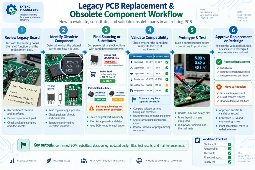
A readable top marking does not always identify a complete manufacturer part number. Package size, pin arrangement, surrounding circuitry, and manufacturer documentation help narrow the possibilities. Unmarked parts and custom devices may remain unresolved.
Keep a BOM with confirmed identities, uncertain entries, and proposed substitutes clearly separated. Do not label a candidate as equivalent just because it fits the footprint. TI’s cross-reference categories show why matching pins alone is not enough. Pin-for-pin replacements can still have different electrical parameters.
Compare operating limits, tolerances, timing, power, thermal behavior, and circuit-specific requirements. Then test the replacement in the actual circuit. A substitution may require layout changes, different surrounding components, or firmware updates. Discuss obsolete component sourcing alongside engineering validation.
Firmware is a separate constraint. Microchip’s memory guidance notes that code protection can restrict programmer or debugger access. Rebuilding copper connections does not recover the program. Obtain an authorized firmware package and programming instructions, or assess a separately authorized software redevelopment effort.
When Reverse Engineering Makes More Sense Than Redesign
Legacy PCB replacement is worth assessing when the existing function still meets the need, the mechanical interfaces must stay unchanged, and enough evidence exists to validate a replacement. It may preserve compatibility with equipment that remains useful.
A broader redesign may be more practical when key parts or firmware are unavailable, the original design has known weaknesses, or new functions are required. Recovering every detail of an old board can offer little value if most of it must change.
Compare both options using total engineering effort, component availability, testing, future maintenance, and any required product requalification. Neither route is automatically cheaper or faster. An engineering design review can help define the technical questions before choosing a route. Resolve the legal basis separately.
A useful first milestone is a feasibility assessment, not an immediate batch order. Ask what can be confirmed from the supplied sample, which unknowns remain, and what additional samples or documents would reduce the risk. Set a review point before committing to further work.
FAQ
Is PCB reverse engineering legal?
It may be lawful for a particular project, but there is no universal answer. Check the source of the board, applicable IP rights, contracts, firmware restrictions, and intended use in each relevant jurisdiction. Owning the physical board alone is not sufficient.
What documentation is needed to authorize a reverse engineering project?
Provide the board’s origin, project purpose, intended deliverables, and records supporting the relevant rights or permissions. Include applicable licenses and restrictions. An authorization letter must come from someone entitled to grant that scope; an NDA alone does not establish it.
How long does PCB reverse engineering typically take?
There is no reliable universal timeline. Layer count, sample condition, hidden connections, unidentified parts, firmware access, and validation all affect the work. Request a staged estimate after review. Separate analysis and design time from prototype fabrication, assembly, testing, and shipping.
Can obsolete components be substituted during reverse engineering?
Often, but each candidate needs engineering review and testing. Check the full part number, package, pinout, ratings, and behavior in the circuit. Some changes require a revised layout or firmware. Keep approved substitutions and validation results under revision control.
Need to Recreate a Legacy Board?
Start with clear photos, board dimensions, the revision, available files, and a description of the required function. Explain the fault or shortage, sample condition, target quantity, and rights or permissions supporting the work. Share sensitive files only through an agreed channel.
Discuss a legacy board project with Benlida to request a feasibility and scope review. Agree on deliverables, unresolved items, test requirements, and responsibilities before committing to manufacture.