

PCB Lead Time Guide — What Affects Prototype and Production Timelines
What Affects PCB Lead Time?
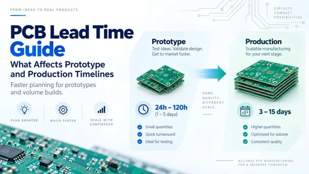
PCB lead time depends on layer count, board construction, material availability, surface finish, and order quantity. Benlida’s reference timings below range from 24 to 120 hours for 2- to 10-layer prototypes. Production timings range from 3 to 15 calendar days. These figures exclude shipping. Confirm their applicability and the start of the lead-time clock in your quotation.
PCB manufacturing lead time covers making the bare circuit board. It does not mean the time until a fully assembled product reaches your team. Component sourcing, assembly, firmware loading, and functional testing belong to the PCBA schedule and need separate planning.
Calendar days include weekends, unlike working days. Still, a duration alone cannot tell you when boards will arrive. Ask for the agreed start point, expected dispatch date, and transit estimate. A delayed design approval or unavailable material can affect the schedule before manufacturing begins.
Prototype Lead Time by Layer Count
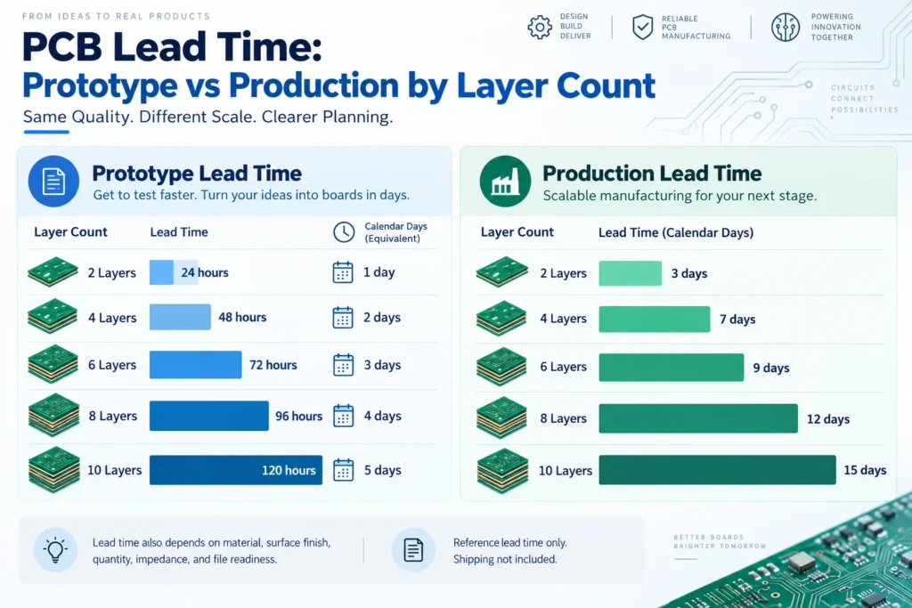
The table gives Benlida’s reference PCB prototype turnaround time by layer count. Hours are continuous elapsed time; the calendar-day column shows the equivalent duration. Shipping is not included.
| PCB layers | Prototype lead time | Calendar-day equivalent |
|---|---|---|
| 2 layers | 24 hours | 1 calendar day |
| 4 layers | 48 hours | 2 calendar days |
| 6 layers | 72 hours | 3 calendar days |
| 8 layers | 96 hours | 4 calendar days |
| 10 layers | 120 hours | 5 calendar days |
Use these timings to start a planning discussion. The quotation must confirm the board construction, prototype quantity, material, finish, and clock start. A layer count by itself does not establish eligibility for a particular turnaround.
Two boards with the same layer count can follow different manufacturing routes. A through-hole design and a design with filled microvias may require different operations. TTM’s overview of HDI structures describes several microvia and lamination approaches. Some use sequential buildup; others use a single lamination cycle. The actual structure matters more than the HDI label alone.
For a first prototype, allow time to answer engineering questions before committing your laboratory schedule. A fast fabrication slot cannot resolve an undefined stackup or conflicting drill files.
Ask which operations drive the schedule for your design. A board with several sequential buildup stages can need more processing than a simpler construction with the same total layer count. Removing unnecessary complexity may help, but only if the revised board still meets its electrical and mechanical requirements.
Production Lead Time by Layer Count
Benlida’s production reference timings are shown below. All durations are calendar days and exclude shipping. Confirm the quantity and construction covered by the quoted schedule.
| PCB layers | Production lead time |
|---|---|
| 2 layers | 3 calendar days |
| 4 layers | 7 calendar days |
| 6 layers | 9 calendar days |
| 8 layers | 12 calendar days |
| 10 layers | 15 calendar days |
A production order may occupy more panels and require a different capacity plan from a prototype lot. Production lead time is not the prototype duration multiplied by the number of boards. Panel layout, batch size, process loading, and inspection requirements all need review.
If your launch depends on an initial batch, ask whether partial shipment is practical. Agree the quantity and date for each shipment, plus any added cost. Do not assume the first batch and the complete order will leave together.
For repeat orders, identify the previously approved revision and highlight every change. A new laminate, finish, or test requirement can make an apparently familiar order different. Reconfirm the schedule when ordering again. A past dispatch date does not reserve capacity for the next batch.
Factors That Extend Lead Time
Surface Finish and Its Process Route
A surface finish protects exposed copper and prepares it for assembly. ENIG, ENEPIG, and OSP use different treatment systems. MacDermid Alpha’s surface-finish guidance explains why selection must consider solderability, assembly needs, and the application.
For scheduling, ask whether the requested finish fits the available process route. There is no universal rule that ENIG adds a fixed number of days or that OSP is always fastest. Do not switch finishes for speed without checking the assembly and reliability requirements.
Special Materials and Copper Requirements
Confirm the exact laminate grade, thickness, copper weight, and stock status before locking the schedule. A material that meets the electrical requirements may still need procurement. An alternative is only useful if engineering approves it and the supplier confirms availability.
Copper requirements also deserve attention. Eurocircuits’ explanation of the copper electroplating process shows how plating time, current density, and copper distribution affect the result. This helps explain why copper specifications need process review. Ask how your copper requirements affect the quoted schedule.
Controlled Impedance and Stackup Approval
Controlled impedance depends on the stackup as well as the routed trace geometry. Polar Instruments’ stackup planning resources combine buildup information with controlled-impedance documentation. A drawing that says only “controlled impedance” leaves important questions unanswered.
Provide the target values, tolerances, relevant layers, and reference planes. Agree how impedance will be verified. If the proposed stackup requires a layout change, resolve it before releasing the final manufacturing files. The main scheduling risk may be the approval loop rather than the measurement itself.
Incomplete Files and Late Revisions
Missing drill data, conflicting board thicknesses, or unclear tolerances can delay engineering review. Use one revision across the fabrication package. State which drawing controls if two documents disagree, and remove obsolete files from the submission.
Changes after approval can require another review or replacement production data. Tell the manufacturer immediately when a revision is necessary. Request an updated schedule instead of assuming the original date still applies.
How to Get Faster PCB Turnaround
Fast PCB production starts with a clear, manufacturable order. Before requesting an expedited option, use the DFM checklist to remove avoidable questions from your fabrication package.
- Send Gerber or ODB++ data, NC drill files, and the fabrication drawing together.
- Specify the layer count, stackup, board thickness, copper requirements, finish, and quantity.
- Identify impedance, special tolerances, inspection records, and other requirements that need review.
- Give the required arrival date and destination, not only a requested manufacturing duration.
- Assign one contact who can approve engineering questions and keep all changes under revision control.
- Ask which approved design or material options could shorten the schedule without changing product requirements.
For flexible boards, ask about fast FPC prototype manufacturing for your exact construction. Include coverlay, stiffener, and bend requirements where relevant. Do not assume the layer-based table automatically applies to every flexible or rigid-flex design.
When requesting an expedite, ask what changes and what stays the same. Confirm the additional charge, accepted quantity, dispatch date, and required inspection scope. A shorter schedule should not depend on silently removing agreed quality checks.
Planning Your Project Timeline Around PCB Lead Time
Work backward from the date the boards must be usable. Keep fabrication, transit, receiving, and any assembly work visible as separate tasks. Our PCB manufacturing services page provides context for preparing the bare-board inquiry.
- Set the required arrival date and allow time for incoming inspection.
- Confirm shipping arrangements and a destination-specific transit estimate.
- Agree the manufacturing duration, its start point, and the expected dispatch date.
- Schedule file preparation, engineering review, and any material procurement against those dates.
- Reserve time for prototype evaluation and a possible design revision before the production release.
For example, the 4-layer prototype reference is 48 hours, or two calendar days. The production reference is seven calendar days. Those figures describe separate builds. They do not include the time your team spends testing the prototype, approving changes, or arranging transport.
Ask whether review and procurement can overlap, and whether either is included in the quoted lead time. This avoids counting the same task twice or leaving it out entirely. Record the agreed dates in writing so engineering, purchasing, and logistics use the same schedule.
A useful order acknowledgment separates the requested date from the accepted date. If the deadline is a laboratory test or assembly booking, tell the supplier why arrival matters. Agree who will report any delay and when you need to know. This gives your team time to adjust downstream work before dispatch.
FAQ
What is the fastest PCB prototype turnaround available?
The shortest timing in Benlida’s reference table is 24 hours for a 2-layer prototype. That is one calendar day and excludes shipping. Confirm your board construction, quantity, material, finish, and clock start before relying on it. It is not a claim that every prototype can be made in 24 hours.
Does surface finish affect PCB lead time?
Yes. The selected finish can change the process route and scheduling options. The effect depends on the finish and the specific order. Ask for the lead time of your approved finish instead of adding a standard number of extra days.
How much faster is prototype lead time compared to production?
In Benlida’s table, a 4-layer prototype takes two calendar days, compared with seven for production. A 10-layer prototype takes five calendar days, compared with fifteen for production. These reference differences are not a universal multiplier. Both schedules exclude shipping and require order-specific confirmation.
Can PCB lead time be expedited for urgent projects?
Ask whether an expedited schedule is available for your files, materials, quantity, and required process route. Availability is not automatic. Confirm any extra cost and revised dates in writing. Keep the agreed inspection requirements in place and check shipping separately.
Confirm the Timeline for Your PCB Project
Send Benlida your fabrication files, quantity, material and finish requirements, and required arrival date. Include the destination and any special inspection needs. Ask for a quotation that confirms manufacturing time in calendar days, the clock start, and shipping separately.