

PCB Rework and Repair — When It’s Possible and When It’s Not
What Is PCB Rework and Repair?
PCB rework and repair can correct assembly defects, replace failed components, and restore some damaged traces or pads. Feasibility depends on the damage, the permitted process, and how the result will be verified. Multiple defects or a lifted pad do not automatically make a board scrap. Replacement is appropriate when an acceptable result cannot be demonstrated.
This guide focuses on populated boards, or PCB assemblies (PCBAs). Rework aims to restore compliance with the applicable drawings and specifications. Repair restores function but may leave a deviation from the original drawings or specifications that needs approval. A board that powers on is not necessarily ready for release.
IPC-7711/7721D provides rework and repair guidance. Select the applicable procedures and acceptance requirements with the engineering and quality teams. The table is a screening aid, not an IPC risk classification or approval to proceed. “Reworkable?” includes repair where stated.
Rework Feasibility
| Defect Type | Reworkable? | Risk Level |
|---|---|---|
| Accessible solder bridge | Often, if pads and components remain sound. | Moderate: heat and pad damage still need control. |
| Failed or incorrect component | Often, with a suitable replacement and intact connections. | Moderate: depends on package and access. |
| BGA solder-joint defect | Potentially, using a qualified rework process. | Higher: hidden joints and thermal exposure. |
| Lifted pad or broken surface trace | Sometimes, through an approved repair. | Higher: adhesion, geometry, and electrical performance. |
| Internal connection damage | Needs specialist assessment; surface repair may not address it. | High: access and verification are difficult. |
| Extensive delamination or charring | Often unsuitable for routine recovery; assess replacement. | Very high: structural or insulation integrity may be compromised. |
Common Rework Operations — Component Replacement, BGA Reballing
PCB component rework may involve correcting a solder bridge, replacing an incorrect part, or removing a failed device. Diagnose the cause first. Replacing a damaged component will not solve an unresolved circuit fault that damaged it.
A controlled BGA rework process generally includes board preparation, device removal, site inspection and cleanup, replacement placement, soldering, and verification. Ball grid array packages have solder connections beneath the body. This makes alignment and inspection more demanding than for readily accessible leads.
Reballing replaces the solder balls on a BGA package. It does not repair damaged silicon or prove that a removed device is suitable for reuse. For example, Analog Devices’ PBGA rework procedure directs users not to reuse removed components. Check the actual device manufacturer’s guidance before considering reballing.
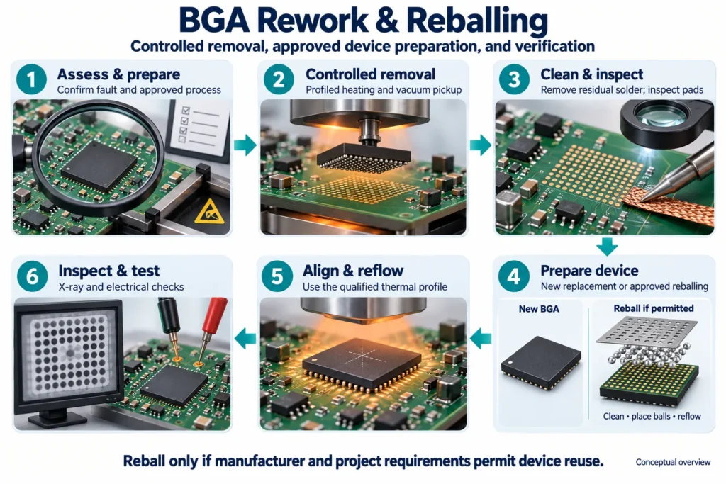
Removal must also preserve evidence when failure analysis is planned. Rough handling or excessive heat can introduce new damage and obscure the original fault. Tell the rework provider whether the removed device must be retained for analysis.
Use X-ray inspection for BGA testing to examine hidden solder features where appropriate. It complements electrical and functional checks; it does not prove the absence of every defect or establish long-term reliability by itself.
Trace and Pad Repair Techniques
Some surface copper damage is repairable. A specialist may replace a damaged conductor section with a suitable copper pattern or use an approved jumper arrangement. The method must match the circuit’s electrical and mechanical requirements.
Circuit Technology Center’s conductor-repair guidance stresses maintaining permitted conductor width, spacing, and current capacity. Restoring continuity alone is insufficient. A high-speed signal path also needs an engineering review of any geometry change.
A lifted or missing pad can sometimes be replaced and bonded to a prepared surface. The same provider’s land-repair procedure explains this approach and its limitations. The supporting board material must be suitable, and the repaired connection may differ from the original construction.
Inspect beyond the visible pad. Damage can involve a plated hole, an internal connection, or the surrounding laminate. A surface patch does not automatically restore those structures.
Document the repair location, materials, approval, and required checks. Confirm both electrical performance and mechanical security before accepting the assembly.
When Rework Is Not Cost-Effective
Technical feasibility and commercial value are separate questions. Compare diagnosis, setup, labor, replacement parts, inspection, and retesting with the cost and availability of a replacement assembly.
A high-value board with one confirmed fault may justify detailed recovery work. A readily available board with uncertain internal damage may not. Several accessible solder defects can be easier to resolve than one inaccessible connection failure.
Before deciding when to scrap a PCB assembly, ask:
- Is the root cause understood, or would the work be trial and error?
- Is the proposed repair permitted by the product and customer requirements?
- Can the repaired area meet its electrical and mechanical requirements?
- Are suitable replacement parts, equipment, and trained personnel available?
- Can the final assembly be tested adequately before release?
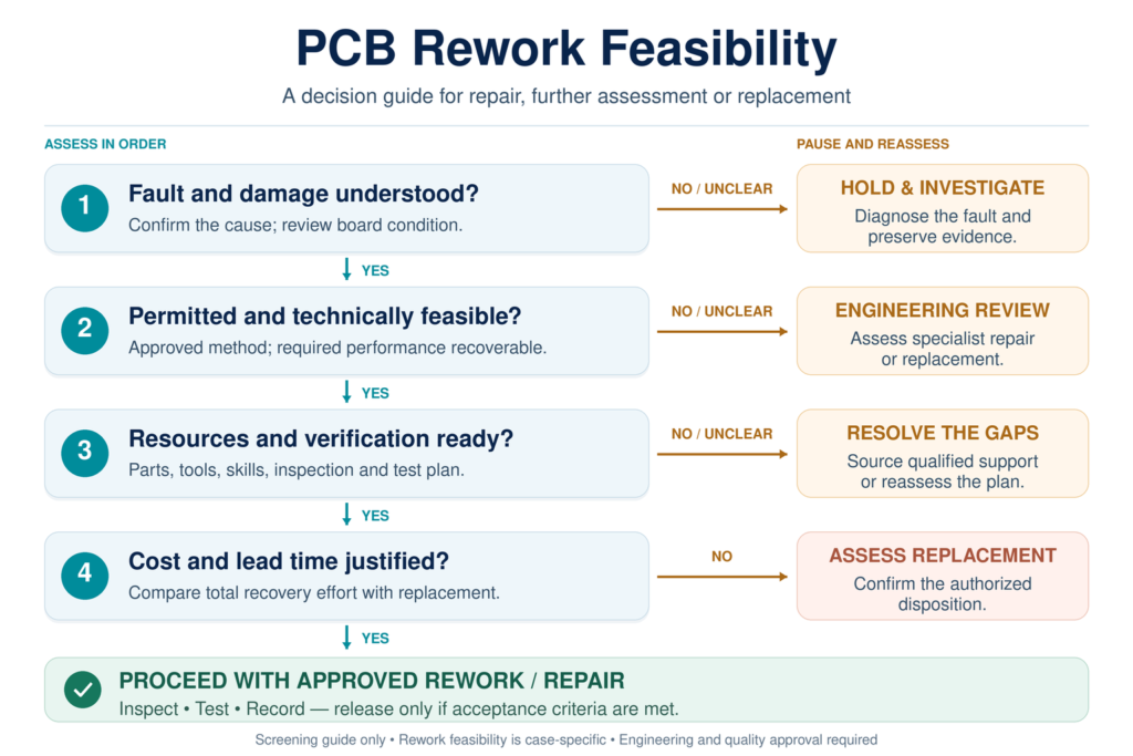
If an acceptable result cannot be established, stop rather than repeat heating attempts. Keep affected units identified and separate until an authorized disposition is recorded. Do not discard a suspect assembly needed for failure analysis without approval.
Rework Risk — Thermal Damage and Delamination
Rework adds heat and handling to an assembly that has already been processed. Excessive exposure can damage packages, lift pads, or distort the board. The target component and nearby parts both need consideration.
Moisture adds another risk. TI’s MagPack rework guidance identifies moisture-induced PCB and device delamination as concerns. Its process examples are specific to those power modules. Package delamination and separation within the PCB laminate are different failure locations. Identify what is damaged before selecting a recovery method.
Review the component limits, board construction, storage history, and previous thermal cycles. Establish a measured profile for the actual assembly. Do not apply a generic baking temperature or heating time to every board.
There is also no universal safe number of rework attempts. IPC-7711/7721D does not set one maximum count for every assembly. That does not permit unlimited heating. Component guidance, material condition, process qualification, and project requirements still govern the decision.
Afterward, inspect the affected area and complete the agreed tests. Record the operation and results against the board’s identity. A passing functional test supports release decisions but cannot alone establish service-life performance.
Preventing Rework Through Better DFM and Inspection
Design for manufacturing starts before the first build. Review footprints, polarity, component clearances, assembly drawings, and revision consistency. Include design-for-assembly and test-access checks, not just bare-board fabrication rules.
Altium’s DFM guide links component spacing with soldering, rework access, and testing. Leave practical access around difficult packages and plan test points with the assembler. Use the PCB DFM checklist to organize the discussion.
Inspection can identify defects earlier, but it does not prevent the process error that caused them. Feed findings back into stencil design, placement, soldering, handling, or documentation as appropriate. Track repeated defects by location and process stage.
When discussing quality control services, define the checks, acceptance criteria, and records needed for your project. Agree how repaired units will be identified and retested. Early review can reduce avoidable rework without promising a defect-free build.
FAQ
Can a BGA component be reworked without damaging the board?
Yes, suitable assemblies can undergo controlled BGA rework. Success depends on the board’s condition, package requirements, equipment, and verified process. Inspect the site and surrounding components afterward. Reusing or reballing the removed device is a separate decision governed by manufacturer and project requirements.
When should a defective PCB be scrapped instead of repaired?
Consider replacement when repair is prohibited, required performance cannot be verified, or recovery is impractical. Extensive structural damage deserves particular caution. Defect count or one damaged pad alone is not a reliable scrap rule. Obtain the required disposition approval.
Does rework affect PCB reliability long-term?
It can. Extra heat, mechanical stress, and repair geometry may affect reliability. A controlled process can reduce these risks, but a board that passes a short test is not automatically proven for its full service life. Validation should match the application.
How can DFM review reduce the need for rework?
DFM review can catch unsuitable footprints, poor clearances, unclear polarity, and incomplete manufacturing data before assembly. Test-access planning helps diagnose faults. Combine these reviews with process controls and inspection feedback; design review alone cannot eliminate every defect.
Dealing with a Defective Board?
Ask about rework options for your project with Benlida. Share the board revision, defect photos, test results, BOM, assembly files, and known rework history. Include the acceptance requirements and affected quantity. Confirm whether assessment, rework, or replacement support is available before sending hardware.