

PCB Layer Count Guide — When Do You Need More Layers?

What Determines PCB Layer Count?
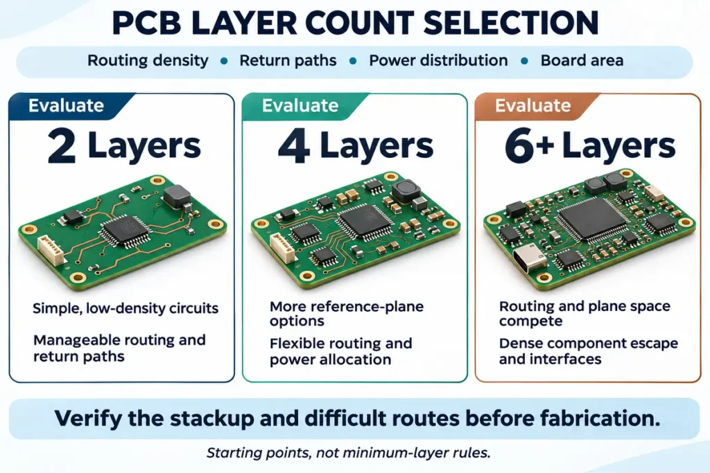
PCB layer count depends on routing density, power and ground requirements, and signal integrity. Two layers can suit simple circuits. Four layers provide more room for reference planes. Dense designs may need six, eight, or more layers. Extra layers usually raise fabrication cost and can affect lead time, but they can also reduce routing compromises.
Layer count means the number of conductive copper layers. It does not include solder mask or silkscreen. Some copper layers carry traces; others serve mainly as power or ground planes. A six-layer board therefore does not necessarily offer six signal-routing layers.
Start with the board outline, component placement, connector positions, and important connections. Ask what is limiting the layout: space for traces, a continuous return path, power distribution, or access to component pads.
Do not judge signal demands from clock frequency alone. TI’s high-speed layout guidance explains the importance of rise and fall times. Even a signal that switches infrequently can have fast edges. Evaluate those edges together with trace length and the device’s layout requirements.
When 2-Layer Boards Are Sufficient
A two-layer PCB is a useful starting point for a simple controller, interface board, or low-density circuit. It works when connections fit without excessive detours and the layout can preserve suitable power and return paths.
Both sides are available for copper, but routing them heavily can leave ground copper fragmented. Check the copper beneath important traces. A ground pour elsewhere on the board does not automatically provide a useful return path for that signal.
Radio-frequency circuitry does not automatically rule out two layers. Espressif’s ESP32 layout guidance recommends four layers but also describes a two-layer option. That option keeps bottom-layer traces limited and preserves ground beneath the chip, RF section, and crystal. These are device-specific conditions, not a universal two-layer recipe.
Before adding layers, try improving placement or allowing more board area. If the design only fits by cutting important ground paths or crowding every connection, compare a four-layer option before committing to fabrication.
When 4-Layer Boards Make Sense
The main benefit in a 2-layer vs 4-layer PCB comparison is the freedom to allocate copper. Internal planes can provide references and power distribution while outer layers carry components and signals.
A familiar example is signal, ground, power, signal. Analog Devices’ mixed-signal layout guide discusses this arrangement. It is a starting point, not the only valid stackup. Some designs use two ground layers and distribute power through traces or copper regions instead.
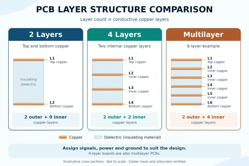
Give each important signal a suitable reference. In the signal/ground/power/signal example, bottom-layer signals may reference the power plane. Splits in that plane and transitions between references need careful review. Simply naming a layer “power” does not solve the return-path problem.
Four layers are worth evaluating when a two-layer layout struggles to keep critical routes short, maintain ground continuity, or distribute power cleanly. They may also help separate noisy switching circuits from sensitive analog circuitry. Good placement and decoupling remain essential.
Choose the layer order and spacing before detailed routing. Our PCB stack-up design guide explains the next planning step.
High-Density Designs Requiring 6+ Layers
Consider six or more layers when routing and plane requirements compete for the same space. Common triggers include dense ball grid array (BGA) packages, several memory or high-speed interfaces, multiple power rails, and a tightly constrained board outline.
Test the difficult connections first. BGA escape routing means getting traces from the package pads into the wider board. If those routes cannot reach usable routing channels, extra space elsewhere may not help.
A practical example appears in TI’s sensor-fusion reference design. Its designers used six layers, adding two to simplify BGA fan-out and routing. This illustrates a design-specific reason for extra layers, rather than a rule for every board with a BGA.
High-density interconnect, or HDI, is a separate decision. Microvias and build-up structures can open routing space without requiring the same total layer count as a conventional design. Würth Elektronik’s HDI stackup examples include four, six, eight, and ten layers. HDI therefore does not mean “six layers or more.”
Compare the complete via structure and manufacturing process. Our HDI PCB design rules guide covers the related design questions.
Layer Count vs Cost and Lead Time Trade-Offs
More layers generally increase fabrication cost when other specifications stay similar. However, there is no fixed price for each added layer. Size, materials, copper weight, via structure, quantity, and tolerances also affect the quotation. These factors appear in Bittele’s PCB manufacturability guide.
The table provides starting points for multilayer PCB selection. Relative cost assumes broadly similar materials, dimensions, quantities, and manufacturing requirements. It is not a quotation or a minimum-layer rule for any application.
Layer Count Guidance
| Layer Count | Typical Use Case | Relative Cost |
|---|---|---|
| 2 | Simple controllers and low-density interfaces with manageable return paths. | Usually lowest. |
| 4 | Moderate routing density with dedicated reference-plane options. | Low to moderate. |
| 6 | Denser processor or mixed-signal boards needing more routing and plane space. | Moderate. |
| 8 | Dense processor, memory, and multiple-interface designs. | Moderate to high. |
| 10 or more | Very dense systems with extensive routing and power-distribution needs. | Higher; depends on construction. |
Manufacturing steps matter as much as the final count. Eurocircuits’ buildup guidance identifies extra press cycles and blind/buried via processing as cost drivers. Adding two copper layers does not automatically add a separate lamination cycle; the selected construction determines the process.
For a useful comparison, request prices for two feasible stackups at the same quantity. Keep material, finish, copper weight, and testing requirements consistent. List any construction changes needed by the lower-layer option. A smaller layer count is not a saving if it requires a more expensive process or another design revision.
Ask for lead time alongside each price. Material availability, order quantity, and special processing also affect the schedule. Confirm when fabrication time starts and whether the quoted schedule includes assembly or shipping. Do not estimate delivery from layer count alone.
Layer Count and Impedance Control Relationship
Layer count does not directly set impedance. Trace width, copper thickness, spacing to reference planes, and dielectric properties determine the structure. For differential pairs, spacing between the traces also matters. Altium’s controlled-impedance documentation describes these relationships.
Two-layer boards can support controlled impedance. However, the required trace geometry may consume too much space for a particular design. More layers can offer closer reference planes and more routing choices. The benefit comes from the resulting geometry, not from the number printed on the fabrication drawing.
Do not copy a trace width from another board without checking its stackup. The same width can produce a different impedance with different materials or reference spacing. Agree on available materials and dimensions with the fabricator before final routing.
Include these details in the review:
- Signal groups, target impedances, and allowed tolerances.
- Routing layers and their intended reference planes.
- Proposed stackup, board thickness, and copper weights.
- Via transitions, connector connections, and any required verification.
An impedance calculation for a straight trace does not validate the complete connection. Check transitions and return paths as part of the circuit review. Add layers when they solve a documented constraint, then verify the revised layout.
FAQ
How do I know if my design needs more than 2 layers?
Review placement, routing space, power distribution, and return paths. If important traces need long detours or repeatedly interrupt ground copper, evaluate four layers. Follow component layout guidance and check the difficult connections early. Component count alone is not enough to decide.
Do more layers always mean better performance?
No. Extra layers provide options, but poor placement, broken reference planes, and unsuitable transitions can still cause problems. Each added layer should serve a clear purpose. Compare the resulting routing and stackup, then verify performance against the actual design requirements.
How much does adding layers increase PCB cost?
There is no universal percentage. The price depends on the complete construction, board size, quantity, and manufacturing requirements. Request comparable quotes for feasible alternatives. Include fabrication, any assembly changes, and expected redesign work when evaluating the total project cost.
What layer count is typical for HDI designs?
HDI has no single required layer count. Four-, six-, eight-, and higher-layer constructions are possible. Choose the structure around component escape routing, microvia requirements, reference planes, and manufacturability. A high-layer-count board is not automatically an HDI board.
Not Sure How Many Layers Your Design Needs?
Benlida’s engineering team recommends layer count based on routing density and signal requirements during DFM review.
Explore our multilayer PCB manufacturing services. Get a layer count recommendation by sharing your board outline, preliminary layout, key interfaces, impedance targets, and order quantity. Include Gerber or ODB++ files, drill data, and a fabrication drawing when available.