

PCB Stack-Up Design Guide — Layer Count, Impedance Control & Material Selection
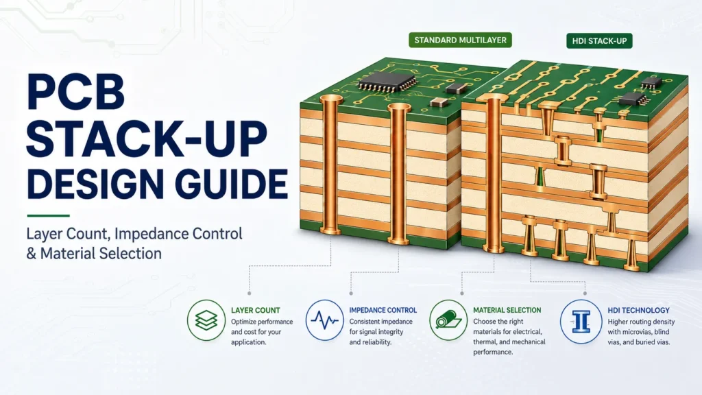
A PCB stack-up defines how copper and dielectric layers are arranged inside a printed circuit board. It affects routing space, signal quality, power delivery, heat flow, board thickness, and manufacturing cost.
A good stack-up defines copper thickness, dielectric thickness, material, layer order, and impedance targets. It must also match the PCB manufacturer’s capabilities.
This PCB stack up design guide covers layer count, layer order, impedance, materials, HDI structures, and common mistakes.
What Is PCB Stack-Up?
A PCB stack-up is the vertical arrangement of conductive and insulating layers in a circuit board. Conductive layers are usually copper. Insulating layers are made from core materials and prepregs.
A core is a cured laminate. A prepreg is a resin-coated glass material that bonds layers during lamination.
The stack-up controls the distance between traces and reference planes. This affects impedance, signal behavior, board thickness, and mechanical balance. For boards with both rigid and flexible sections, use the rigid-flex stack-up design guide.
Plan the stack-up before detailed routing. Late changes can affect trace width, vias, and layer assignments.
Engineers can review general printed board design requirements through the IPC design standards. Final values should still be confirmed with the selected fabricator.
How to Choose the Right Layer Count
More layers provide more routing space and more reference planes. They can improve signal integrity and power distribution. They also increase manufacturing steps and cost.
Choose the lowest layer count that meets the electrical, mechanical, routing, and reliability needs of the product. Do not select a layer count based only on board size.
| Layer Count | Typical Use Cases | Main Advantages | Main Limits |
|---|---|---|---|
| 2 layers | Simple controllers, LED boards, low-density consumer products, basic power circuits | Low cost, short lead time, easy inspection | Limited routing space and weak reference-plane control |
| 4 layers | Industrial controls, communication modules, compact embedded systems, moderate-speed digital boards | Dedicated ground and power planes, better return paths, improved EMC performance | Limited internal routing and fewer options for complex power domains |
| 6 layers | High-speed interfaces, dense mixed-signal boards, advanced industrial electronics | More routing channels, better plane placement, stronger signal isolation | Higher fabrication cost and more stack-up decisions |
| 8 layers | Network equipment, computing hardware, medical electronics, dense BGA designs | Multiple reference planes, better power distribution, more controlled routing | Higher cost, tighter material control, and more complex via planning |
Two-layer boards suit simple circuits. Four-layer boards add dedicated planes and better return paths. Six-layer and eight-layer boards offer more routing space and stronger plane control. Benlida supports multilayer PCB manufacturing for these structures.
Signal Layer Arrangement Rules
Layer order is as important as layer count. A poor order can create long return paths, crosstalk, and unstable impedance.
Place High-Speed Signals Next to a Solid Reference Plane
A fast signal needs a continuous return path on a nearby reference plane. Keep high-speed signal layers close to solid ground planes to reduce loop area.
Avoid Routing Across Plane Splits
Do not route a critical signal over a plane gap. When a signal changes layers, add a nearby stitching via when the reference plane also changes.
Keep Power and Ground Planes Close
A closely spaced power-ground pair can add distributed capacitance and help reduce power noise.
Use a Mechanically Balanced Construction
Balance copper and dielectric construction around the board center. Copper weight, core thickness, prepreg thickness, and copper coverage all affect bow and twist.
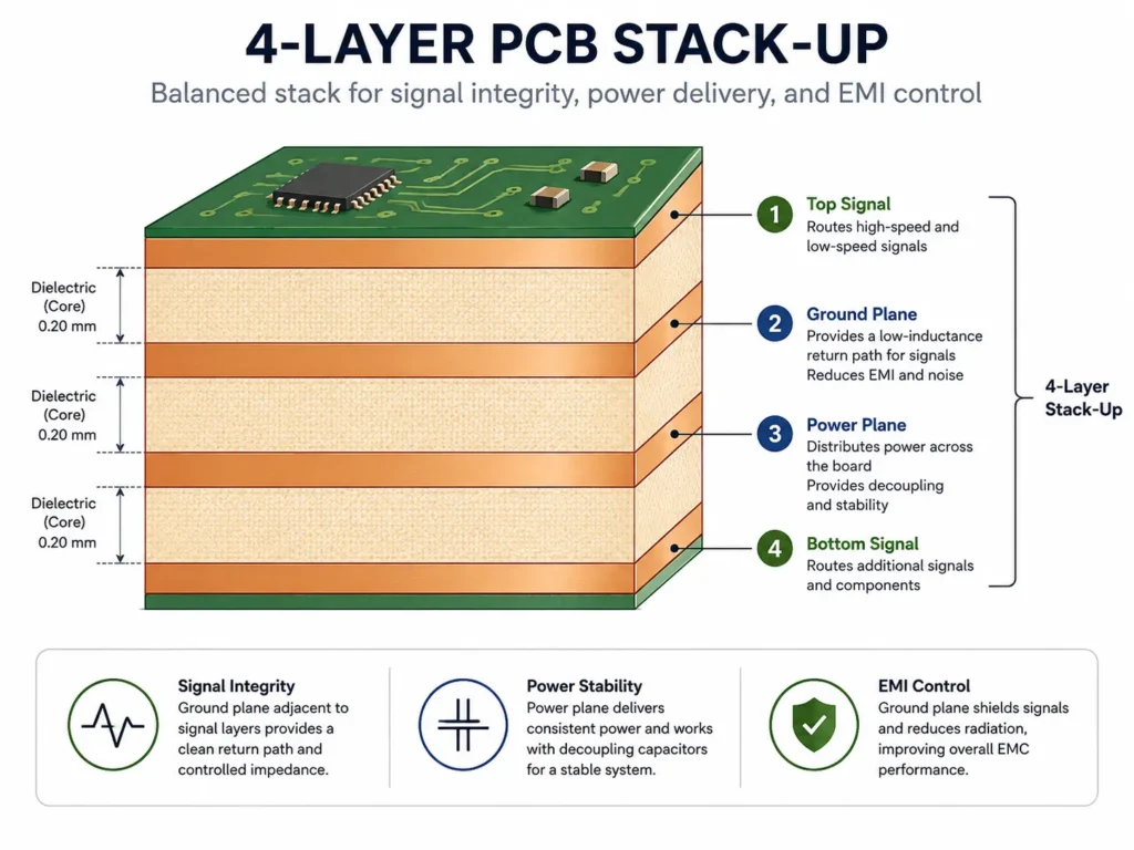
Example Four-Layer Arrangement
- Layer 1: Components and signals
- Layer 2: Solid ground plane
- Layer 3: Power plane and low-speed routing where allowed
- Layer 4: Components and signals
This arrangement gives Layer 1 a close ground reference. The final order should match routing density, power needs, and EMC targets.
Impedance Control in PCB Stack-Up
Controlled impedance is needed when a trace behaves like a transmission line. This includes many high-frequency signals and digital signals with fast edges.
Common targets include 50-ohm single-ended traces and 90-ohm or 100-ohm differential pairs. Always follow the interface specification.
Microstrip
A microstrip is usually an outer-layer trace above a reference plane. It is easy to inspect, but solder mask and the surrounding air can affect impedance.
Stripline
A stripline is an internal trace between reference planes. Its field stays mainly inside the board, which improves shielding. It also needs tight manufacturing control.
What Controls Trace Impedance?
- Trace width
- Copper thickness
- Distance from the trace to the reference plane
- Dielectric constant of the laminate
- Trace shape after etching
- Solder mask and surface treatment
- Differential pair spacing
Equations provide an early estimate. Final values should use a field solver with actual material data. The manufacturer may adjust trace width to reach the target after processing.
Include the impedance target, tolerance, reference layer, and test coupon requirement in the fabrication notes. A complete DFM stack-up review can identify conflicts before production.
Dielectric Materials for PCB Stack-Up
Material selection affects electrical performance, reliability, lead time, and cost. Review the full laminate data, not only the material name.
FR-4 Materials
FR-4 is a broad family of glass-reinforced epoxy laminates. It supports many industrial, consumer, communication, and power products.
Ask for the actual material brand and data sheet. Check dielectric constant, dissipation factor, glass transition temperature, and z-axis expansion.
Low-Loss and High-Frequency Materials
RF, microwave, antenna, radar, and very high-speed designs may need lower-loss materials with tighter dielectric control.
Rogers offers several high-frequency laminate families. Its RO4003C laminate information describes controlled dielectric properties and low-loss performance.
Before replacing FR-4, review drilling, bonding, lamination, and other fabrication needs.
Hybrid stack-ups combine different material families. They can reduce cost when only some layers carry RF signals. They can also create bonding and thermal expansion challenges. Use a fabricator with proven experience in high frequency PCB production.
Material Availability Matters
Confirm available cores, prepregs, copper weights, and finished thicknesses before routing. A replacement with the same nominal dielectric constant may still differ in loss, glass weave, and tolerance.
HDI Stack-Up Design
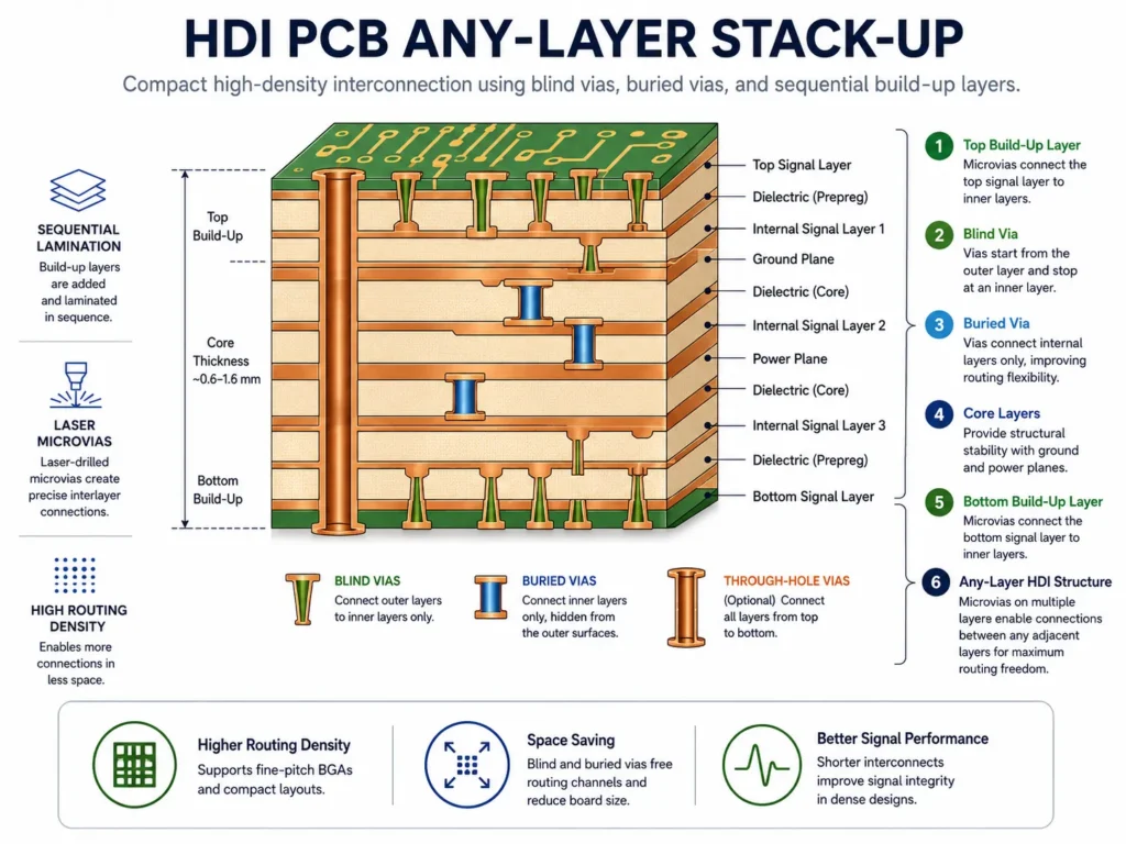
HDI boards use microvias, fine traces, and thin dielectrics. They can reduce board size and improve routing around fine-pitch BGAs. Via structure affects lamination cycles, reliability, and cost.
1+N+1 Structure
A 1+N+1 stack-up has one build-up layer on each side of a central core. It suits designs that need one microvia step to reach the core.
2+N+2 Structure
A 2+N+2 stack-up has two build-up layers on each side. It offers more routing depth and may use stacked or staggered microvias. Confirm filling and stacking limits with the manufacturer.
Any-Layer HDI
Any-layer HDI uses microvias between many or all adjacent layers. It offers strong routing freedom but may require several lamination cycles. Use it only when density justifies the added cost.
IPC lists a dedicated design standard for HDI boards. The supplier should also provide a capability table and preferred structures.
Benlida supports HDI PCB fabrication. Share the BGA pitch, via structure, impedance targets, and finished thickness during the early review.
Common PCB Stack-Up Mistakes
Starting the Stack-Up After Routing
Routing before stack-up approval creates rework. Set a preliminary stack-up and confirm it before locking the layout.
Using an Asymmetric Construction
An unbalanced stack-up can increase bow and twist. Balance dielectric thickness, copper weight, and copper coverage around the center.
Ignoring Prepreg and Core Availability
Do not specify unavailable dielectric thicknesses. Confirm material combinations, resin content, and pressed prepreg thickness.
Routing High-Speed Signals Without a Continuous Reference
Review the return path for every critical interface. Avoid plane splits and add return vias near layer transitions.
Requesting Controlled Impedance Too Late
Late impedance requests may force new trace widths, spacing, or layer count. Define targets early and add them to the fabrication drawing.
Choosing HDI Without a Clear Routing Need
Use HDI to solve a real density problem. First check whether standard blind vias or a higher layer count can solve it at lower risk.
PCB Stack-Up Design Checklist
- Confirm board thickness and thickness tolerance.
- Choose the layer count from routing and electrical needs.
- Place critical signal layers next to solid reference planes.
- Keep the physical construction balanced.
- Define copper weight for every layer.
- Define single-ended and differential impedance targets.
- Confirm actual core and prepreg options with the manufacturer.
- Review via spans, microvia stacking, and lamination cycles.
- Check the return path across layer transitions.
- Add test coupon and impedance tolerance requirements.
- Approve the production stack-up before final routing release.
Frequently Asked Questions About PCB Stack-Up Design
What is the main purpose of a PCB stack-up?
The stack-up defines the order and thickness of copper and dielectric layers. It creates routing space and reference planes. It also controls impedance, board thickness, mechanical balance, and manufacturing requirements.
How many layers should a PCB use?
Use the lowest layer count that meets routing, signal integrity, power delivery, EMC, and mechanical needs. Simple circuits may use two layers. Dense or high-speed designs often need four, six, eight, or more layers.
What is the difference between microstrip and stripline?
A microstrip is usually an outer-layer trace above a reference plane. A stripline is an internal trace between reference planes. Stripline provides better field containment. Microstrip is easier to access and inspect.
When should an engineer use an HDI stack-up?
Use HDI when fine-pitch components, limited board area, or high routing density cannot be handled by standard through-hole vias. Confirm the microvia and sequential lamination structure with the manufacturer before layout.
Review Your PCB Stack-Up Before Production
A reliable PCB begins with a manufacturable stack-up. Send your layer plan, board thickness, copper weight, impedance targets, material needs, and via structure to Benlida.
Get a stack-up review before you release the final Gerber or ODB++ files. Early review can reduce layout changes, material substitutions, and production delays.