HDI PCB Design Rules: Vias, Trace Spacing, and Stack-Up
HDI PCB design rules coordinate microvia geometry, trace width and spacing, capture and target lands, copper thickness, and the sequential-lamination stack-up. Frequently discussed planning values include 3/3 mil trace and space, about 0.10 mm laser microvias, and a microvia depth-to-diameter ratio near 0.8:1. These are not universal IPC limits. Freeze the stack-up and use the selected fabricator’s qualified rules before routing.
Each rule affects the others. A smaller via needs a suitable dielectric thickness and land size. A finer trace can limit finished copper thickness. Early alignment prevents a dense layout from becoming difficult or costly to build.
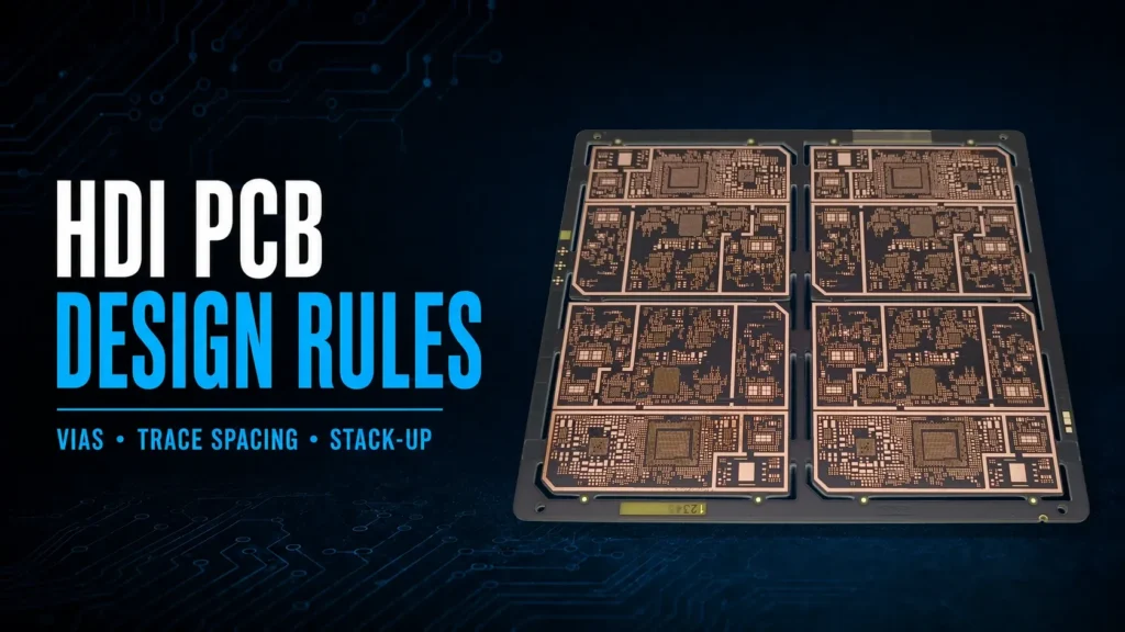
What Are HDI PCB Design Rules?
High-density interconnect, or HDI, uses microvias, fine conductors, and build-up layers to route dense packages. Its rules connect the layout to the selected materials, manufacturing process, inspection plan, and performance requirements.
Start with the component escape pattern and layer connections. Define the stack-up, lamination sequence, via spans, dielectrics, copper weights, and impedance targets. Then lock the trace, clearance, pad, and via rules.
Standards do not replace a supplier capability table. IPC’s current document revision table lists IPC-2226A as no longer maintained and IPC-6016 as superseded. IPC-2226 can still offer historical HDI guidance. IPC-6012F is the current rigid-board performance specification and expands microvia reliability requirements. Purchase documents should name the applicable standard, revision, performance class, and project-specific criteria.
Microvia Structures and Design Rules
A microvia is a small blind connection in an HDI build-up. It is usually laser drilled through a thin dielectric to an adjacent layer. Mechanical drilling remains useful for larger through holes and buried vias. These are separate interconnect structures, not types of laser microvia.
Stacked and staggered describe alignment across build-up layers. They are arrangements, not drilling methods. The choice depends on routing density, lamination, fill, reliability, and supplier experience.
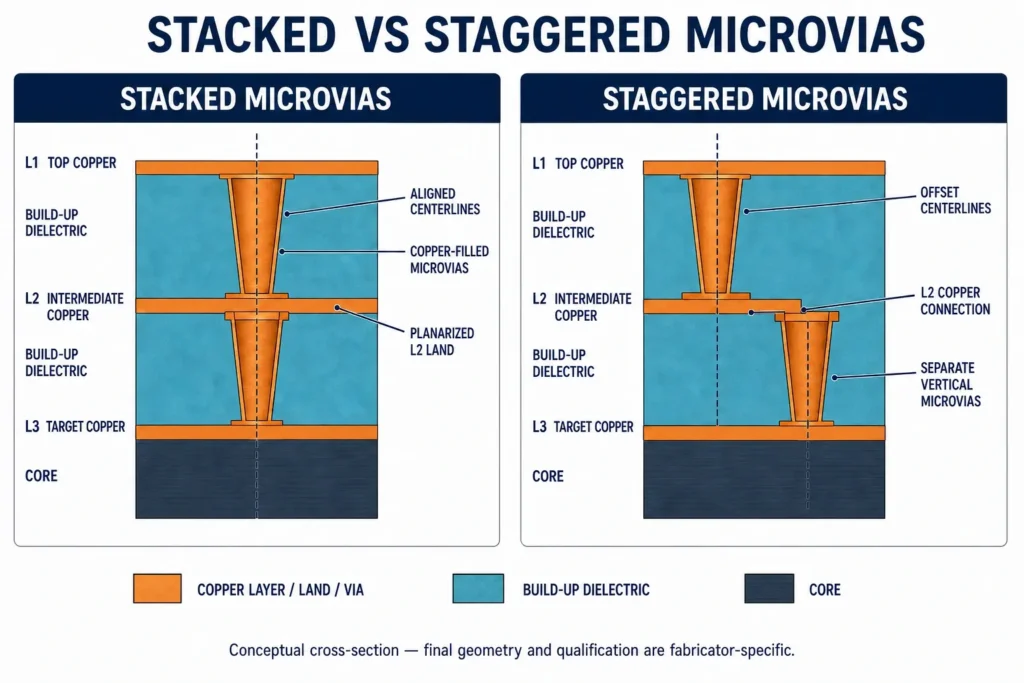
HDI via structure comparison
| Structure | How It Is Built | Typical Use | Main Design Check |
|---|---|---|---|
| Single blind microvia | Usually laser drilled from an outer layer to the next copper layer | Fine-pitch component escape and short layer transitions | Diameter, dielectric depth, target land, and registration |
| Staggered microvias | Adjacent microvias are offset on successive build-up layers | Multi-layer connections with less direct vertical interface stacking | Enough routing area between the offset lands |
| Stacked microvias | Filled microvias are placed vertically above one another | Dense vertical connections when lateral space is limited | Via fill, planarization, copper interfaces, and reliability qualification |
| Mechanical buried or through via | Drilled before or after selected lamination stages, depending on the span | Longer layer connections, power routing, or mixed HDI structures | Drill aspect ratio, annular ring, and a buildable lamination sequence |
Stacked microvias save area but need extra care. An IPC industry warning on microvia reliability describes latent failures at weak interfaces in some stacked, filled structures. It does not say every stacked design will fail. Agree on materials, stack height, process qualification, test coupons, and application-specific reliability testing.
For a broader view of plated through holes, blind vias, buried vias, and via-in-pad, see Benlida’s guide to PCB hole types and applications.
Trace and Space Requirements
Trace width and spacing depend on more than the artwork. Base and finished copper, plating, impedance, etching, and inspection criteria affect the workable rule. Inner and plated outer layers may need different values.
Designers may use 3/3 mil and 2/2 mil as early comparison points. These are not IPC categories. Würth Elektronik’s ADVANCED.hdi design rules, for example, show 75/75 and 50/50 micrometers for two levels of one qualified technology. Other suppliers may use different limits and materials.
Illustrative HDI process windows, not universal IPC limits or verified Benlida capabilities
| Planning Tier | Trace / Space Example | Laser Microvia Example | Aspect-Ratio Approach | Build-Up Scope |
|---|---|---|---|---|
| Selected HDI process example | About 3/3 mil (75/75 µm) or wider | About 0.10 to 0.125 mm | Target 0.8:1 or lower where practical | Often one build-up layer per side; supplier-qualified options may go further |
| Advanced HDI planning | About 2/2 mil (50/50 µm) | About 0.07 to 0.10 mm | Still based on the qualified process, not automatically a higher ratio | May use multiple sequential layers or an any-layer construction |
These are planning examples, not a Benlida capability statement or universal minimum. Ask for separate inner-, outer-, and neck-down rules. Also confirm whether quoted dimensions are designed, drilled, or finished.
How to Calculate Microvia Aspect Ratio
Microvia aspect ratio compares the via depth with its diameter. A lower ratio is generally easier to plate than a deeper hole of the same diameter.
Aspect ratio = via depth ÷ applicable finished via diameter
Laser vias may taper. Ask whether the fabricator uses the minimum finished diameter or another controlled value. A 1:1 ratio is often treated as an upper microvia boundary, while 0.7:1 to 0.8:1 is commonly preferred. The qualified limit still controls.
Illustrative microvia depths at a 0.8:1 depth-to-diameter ratio
| Via Diameter | Example Depth at 0.8:1 | Design Meaning |
|---|---|---|
| 0.075 mm | 0.060 mm | Advanced geometry that needs early supplier confirmation |
| 0.100 mm | 0.080 mm | Common planning example for a thin build-up dielectric |
| 0.125 mm | 0.100 mm | A larger target that may allow a thicker dielectric |
| 0.150 mm | 0.120 mm | Still requires plating and land checks for the chosen process |
These depths are calculations, not manufacturing guarantees. Resin flow, copper topography, glass style, and pressed thickness can change the finished geometry. Use the fabricator’s released stack-up for the final check.
HDI Stack-Up Configurations
HDI notation describes build-up layers around a core section. N represents the copper-layer count in the central section. Review the lamination sequence too. The same label can use different materials, via spans, and buried-via processes.
1+N+1 HDI
A 1+N+1 stack-up has one build-up layer on each side of an N-layer core. Microvias connect each outer layer to the adjacent layer. The board may also use plated through vias, while the core may contain buried vias. This works when one microvia transition per side supports package escape.
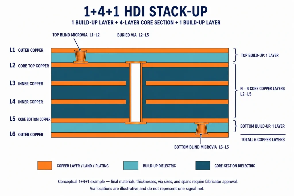
2+N+2 HDI
A 2+N+2 stack-up adds two build-up layers on each side. It supports more routing near dense components but needs more sequential processing. Connections can use staggered or qualified stacked microvias. Freeze every via span before layout.
Any-Layer HDI
Any-layer HDI uses microvias throughout the build-up so signals can move between adjacent layers. It offers routing freedom and reduces through-hole blockage. It also raises material, registration, filling, lamination, inspection, and reliability demands. Approve the construction before layout.
Use Benlida’s PCB stack-up design guide to review layer functions, impedance, and material choices. Then compare the proposed construction with the selected HDI PCB manufacturing process. Public capability pages are a starting point. A project-specific approval is still needed.
Pad and Annular Ring Requirements
A microvia needs an entry capture land and a target land. Their sizes depend on via diameter, registration, dielectric, copper, imaging, and supplier process. No minimum annular ring fits every HDI board.
Nominal annular ring = (land diameter − via diameter) ÷ 2
This is nominal geometry. It excludes registration shift and breakout criteria. Confirm the designed land and required finished condition. Teardrops can help some transitions but cannot repair an undersized target land.
Via-in-pad can shorten escape routing. Under solderable BGA or QFN pads, an open via can draw solder or release gas during reflow. The package guideline may require filling, planarization, and copper plating over the via. Stacked microvias also need a filled, planarized landing structure. State all fill, cap, and acceptance requirements.
Common HDI Design Mistakes
- Routing before the stack-up is approved. This can create invalid via spans or force a late layer redesign.
- Using one supplier’s sample values as universal rules. Fine-line, pad, and microvia limits are process-specific.
- Making the dielectric too deep for the microvia diameter. A high aspect ratio can make plating more difficult.
- Using capture or target lands without registration margin. Nominal overlap alone does not show the finished condition.
- Leaving solderable via-in-pad features open. This may create solder loss, dimples, voiding, or outgassing.
- Stacking many microvias without qualification. More interfaces increase the need for process control and reliability evidence.
- Ignoring finished copper thickness. Extra plating can change trace width, spacing, and impedance.
- Sending incomplete drill information. Every blind, buried, stacked, filled, and capped span must be clear.
Files to Send for an HDI DFM Review
A useful HDI review needs more than Gerber files. Send a consistent package that includes:
- Gerber or ODB++ data and NC drill files.
- A stack-up drawing with layer names, materials, dielectric thicknesses, and copper weights.
- A via table showing start and stop layers, hole sizes, lands, fill, and cap requirements.
- Controlled-impedance targets with trace layers and reference planes.
- Critical component land patterns and package-vendor recommendations.
- Finished board thickness, surface finish, solder mask, outline, and special tolerances.
- Applicable performance, inspection, test-coupon, and reliability requirements.
- Revision identifiers that match across every fabrication file.
Mark every rule that is tighter than the supplier’s normal process. Ask for a written response to open items. A project-specific PCB engineering review should confirm the HDI stack-up and manufacturing rules before release.
HDI PCB Design Rules FAQ
What Is the Minimum Microvia Size for an HDI PCB?
There is no universal minimum microvia size. About 0.10 mm is a useful early planning value, while some qualified processes use smaller diameters. The available size depends on dielectric depth, laser and plating processes, target land, material, registration, and reliability requirements. Confirm both designed and finished dimensions with the fabricator.
What Is the Difference Between Any-Layer and Sequential HDI?
Sequential HDI is a broad manufacturing approach that adds build-up layers through repeated lamination. A 1+N+1 or 2+N+2 board is a sequential HDI construction. Any-layer HDI extends adjacent-layer microvia connectivity through the build-up. It gives more routing freedom but normally needs tighter process control and earlier supplier involvement.
What Aspect Ratio Should an HDI Microvia Use?
A depth-to-diameter ratio near 0.8:1 or lower is a common planning target. A 1:1 ratio is often treated as an upper boundary for microvias. Neither number guarantees manufacturability. Hole taper, material, plating, copper thickness, and the supplier's qualified process determine the accepted rule.
Can HDI Microvias Be Stacked?
Yes. Stacked microvias support dense vertical connections across build-up layers. The lower microvia usually needs to be filled and planarized before the next structure is formed. The design must control the copper interfaces, stack height, land sizes, and reliability plan. Staggered vias may be a simpler option when routing area allows.
What Is the Minimum Annular Ring for an HDI Microvia?
No single annular-ring value applies to every HDI process. The required capture and target lands depend on microvia diameter, registration tolerance, material, copper thickness, and acceptance criteria. Use the component land pattern and fabricator-approved dimensions. Check the worst-case finished result, not only the nominal CAD ring.
Need Help Reviewing an HDI PCB Design?
Planning an HDI PCB? Share your stack-up, Gerber or ODB++ data, drill files, BGA pitch, copper requirements, impedance targets, quantity, revision, and via fill instructions. Benlida can review manufacturability, confirm the available process window, and prepare a project-specific PCB quote.

