SMT Component Package Types — A Guide for PCB Designers
SMT component packages define a device’s physical form and how it connects to the PCB. Common types include rectangular chip components, QFN, QFP, BGA, SOT, and SOIC. Each creates different demands for PCB footprints, solder paste printing, placement, inspection, and rework.
Choose a package by checking the complete part number and its drawing, not just its family name. A smaller body can save space, but fine connections or hidden solder joints may require more planning.
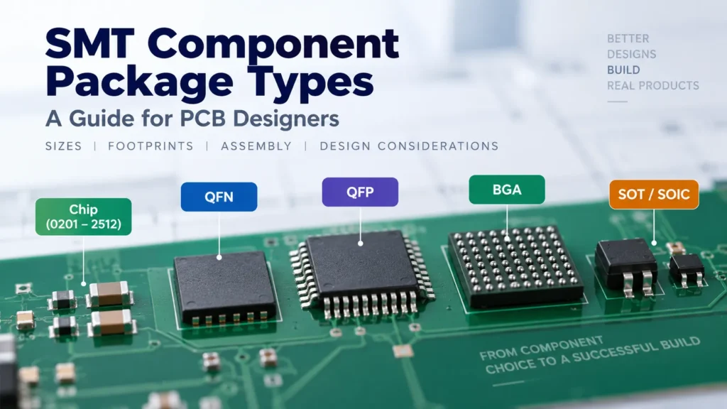
What Are SMT Component Package Types?
SMT means surface-mount technology. An SMD is a surface-mount device: a component mounted on the board surface during assembly. The unpopulated PCB becomes a PCBA after components are assembled onto it.
A component package and a PCB footprint are different. The package drawing describes the physical device. The footprint, or land pattern, defines the board pads and associated layout features needed to mount it.
Package names describe a family, but they do not specify every dimension. For example, two QFN devices can differ in body size, terminal count, pitch, and exposed-pad shape. Pitch means the center-to-center distance between adjacent leads or solder balls.
Before selecting a library footprint, match its dimensions and pin numbering to the exact device. Also check the drawing view. A bottom-view package drawing must not be mistaken for the top view used in your layout.
Passive Component Package Sizes
Chip resistors and many other passive components use numeric size codes. Always identify the coding system. Here, 0201 means the imperial code, represented by a 0.60 × 0.30 mm body. The corresponding metric code is 0603. A metric 0603 must not be confused with an imperial 0603.
The table uses representative nominal body dimensions from Vishay’s CRCW0201 data sheet and D/CRCW chip resistor data sheet. It is a size reference, not a footprint library. Uses are illustrative, and assembly difficulty describes relative process concerns.
| Package (Imperial) | Body Dimensions (L × W, mm) | Common Use Examples | Assembly Difficulty |
|---|---|---|---|
| 0201 | 0.60 × 0.30 | Dense signal and bias circuits | More sensitive to paste volume and placement variation |
| 0402 | 1.00 × 0.50 | Compact resistor circuits | Small pads need controlled printing and placement |
| 0603 | 1.55 × 0.85 | General-purpose signal and bias resistors | Less placement-sensitive than smaller chip sizes |
| 0805 | 2.00 × 1.25 | General resistor circuits and prototypes | Easier handling; pad and paste design still matter |
| 1206 | 3.20 × 1.60 | Resistor positions needing more thermal margin | Easier handling; check heat distribution during soldering |
| 1210 | 3.20 × 2.50 | Larger resistor options where space permits | Check paste deposits and local thermal conditions |
| 2010 | 5.00 × 2.50 | Power-related resistor positions | Larger pads need an appropriate soldering process |
| 2512 | 6.30 × 3.15 | Resistors selected for higher dissipation requirements | Check heating, cooling, and nearby component clearance |
Other series can have different dimensions under the same size code. For example, simplified charts may show different rounded values for 0603 or 2512. Use the exact drawing, including tolerances, height, and terminal dimensions, when building the footprint.
Chip resistor sizes do not establish universal power ratings. Check the chosen resistor’s rating and derating conditions. Likewise, a capacitor with the same size code is not automatically interchangeable in height, land pattern, or electrical performance.
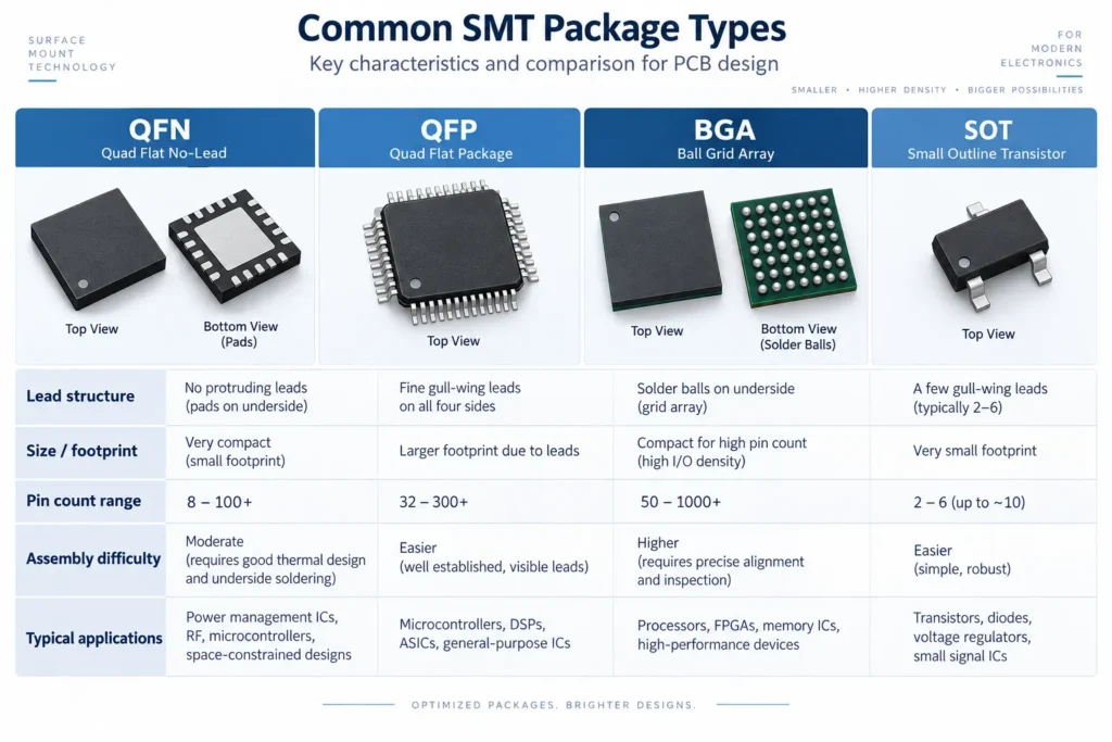
QFN vs QFP Packages
QFN means quad flat no-lead. It has terminals around the underside perimeter rather than long leads projecting from the body. QFP means quad flat package. It uses outward-projecting, gull-wing leads on four sides.
QFN can reduce the board area occupied by connections. Many variants also have an exposed pad underneath for thermal or electrical connection. Follow the device instructions for that pad; do not assume it always connects to ground.
QFN assembly needs careful coordination of land geometry, solder paste, and any thermal vias. Excess or uneven paste can affect seating and solder joints. TI’s QFN and SON attachment guidance explains why pad and stencil design must be considered together. Its example dimensions should not be copied to unrelated parts.
QFP leads are more accessible for optical inspection and some rework operations. However, fine-pitch leads can be bent during handling or bridged during soldering. Visible leads do not make every QFP easy to assemble.
When comparing QFN vs QFP, check the actual pitch, footprint area, thermal needs, and inspection access. The package family alone does not determine which option will be cheaper or more reliable.
BGA Packages
BGA means ball grid array. Solder balls form connections beneath the package, allowing connections across an area rather than only around its edges. BGAs are used in devices such as processors, memory, and programmable logic.
Ball pitch matters because the PCB must route signals away from the pads. A tighter pitch can constrain trace spacing and via placement. Review the ball map and escape routing before fixing the layer stack. Not every BGA requires microvias or the same board construction.
Most BGA joints are hidden from normal optical inspection. Infineon’s BGA assembly recommendations explain how X-ray inspection can reveal features such as solder bridges and voids. They also note that some broken joints are difficult to detect.
Agree on the inspection method and acceptance criteria for the project. X-ray inspection for BGA complements electrical and functional tests; it does not replace them. Leave enough surrounding clearance for the planned inspection and rework approach.
SOT and SOIC Packages
SOT means small outline transistor, but the family also contains packages used for diodes, regulators, and other devices. SOT-23 is a familiar example. SOT does not mean that every device has three pins or the same pinout.
SOIC means small outline integrated circuit. These packages generally have gull-wing leads along two opposite sides. They appear in analog, logic, interface, and other IC products.
Check the exact variant, including lead count, body width, lead span, and pitch. A footprint labeled only “SOIC-8” may not identify the required body width or pad geometry. Analog Devices’ leaded-package design guidance directs designers to the drawing for the specific package code.
External leads can help inspection and probing, but leave room to reach them. Also verify pin 1, device orientation, and the electrical pinout before approving a substitute component.
Package Selection and Assembly Difficulty
Small bodies, fine pitch, and hidden joints create different manufacturing challenges. Compare these features separately instead of assigning one difficulty level to an entire package family.
Small passives generally provide less room for printing and placement variation. Fine-pitch ICs require consistent pad alignment and solder separation. A larger package with closely spaced leads can demand more care than its body size suggests.
Placement accuracy is only part of the process. Stencil thickness, aperture design, solder paste, and board support also influence the result. A board mixing tiny chips with larger thermal pads may need a carefully developed printing process.
Review these questions during component selection:
- Does the exact footprint match the approved part and its pinout?
- Can the PCB route the connections without unnecessary layer or via complexity?
- Can the assembly process handle the package mix and component supply format?
- How will hidden joints be inspected, and what tests verify circuit operation?
- Is there space for rework tools, and are suitable replacement parts available?
Compare total project cost, not just component price. A smaller package may reduce board area but increase routing, inspection, or rework effort. Conversely, a compact part already supported by an established process may be economical. Request a project-specific assessment rather than assuming a fixed price premium.
The PCB assembly process connects printing, placement, soldering, and verification. When discussing SMT assembly services, identify the smallest chips, finest pitches, and hidden-joint packages in your design. Ask the assembler to confirm suitability before the layout is frozen.
FAQ
What is the smallest standard SMT component size?
There is no single smallest size across every component family. Imperial 0201 is only the smallest size in this table. Smaller parts exist: Murata’s small RF inductor mounting guide includes 01005 parts measuring 0.4 × 0.2 mm. Confirm the coding system and the assembler’s support for the exact part.
Why is BGA inspection more difficult than QFP inspection?
BGA solder joints sit beneath the package, so conventional optical inspection cannot see the complete array. QFP’s external leads are more accessible. X-ray can reveal selected hidden-joint defects, but a complete verification plan may also require electrical and functional testing.
What is the difference between QFN and QFP packages?
QFN uses terminals around the underside perimeter, while QFP has projecting gull-wing leads on four sides. QFN can save connection area; QFP can improve access to external joints. Compare exact dimensions, pitch, exposed-pad requirements, and assembly methods rather than choosing by the acronym alone.
Does component package size affect PCB assembly cost?
Yes, but size is only one factor. Fine pitch, printing needs, inspection, rework, and production quantity also influence cost. Smaller components are not automatically more expensive to assemble. Compare the complete PCB and assembly requirements for each option.
Discuss Package Choices Before Finalizing Your PCB
Share your BOM with exact manufacturer part numbers, package drawings, and the current PCB layout or manufacturing files. For an assembly review, include placement data, assembly drawings, and relevant test requirements. Highlight uncertain footprints or proposed component alternatives.
with Benlida to review project suitability. Confirm package-specific assembly, inspection, and rework requirements before committing the design to production.

