PCB Assembly Process — Step-by-Step Guide from Solder Paste to Testing
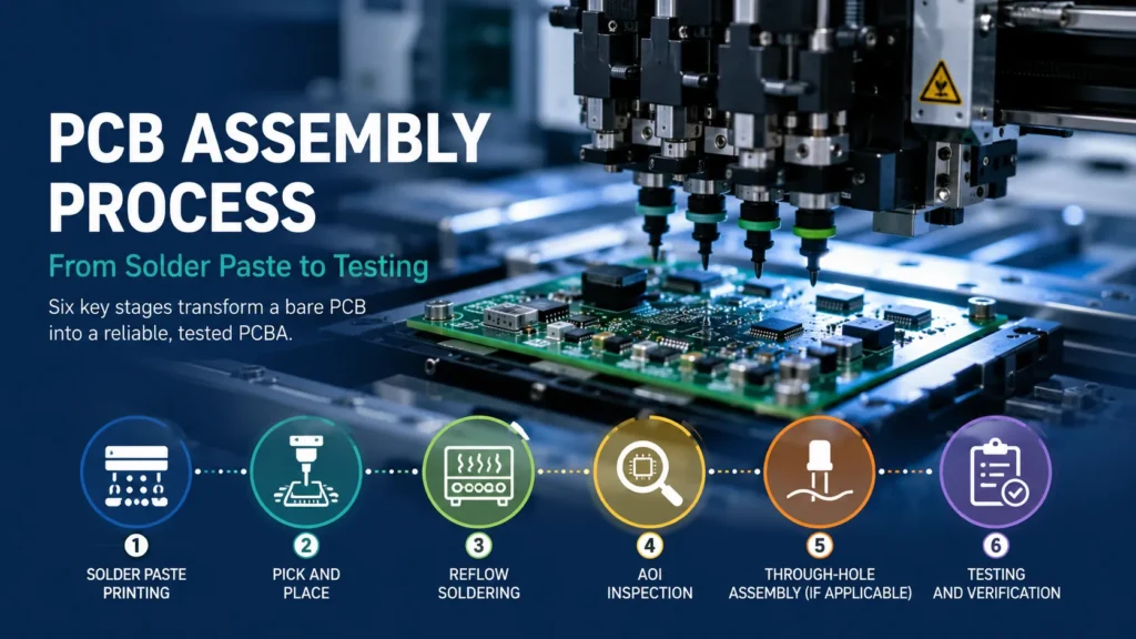
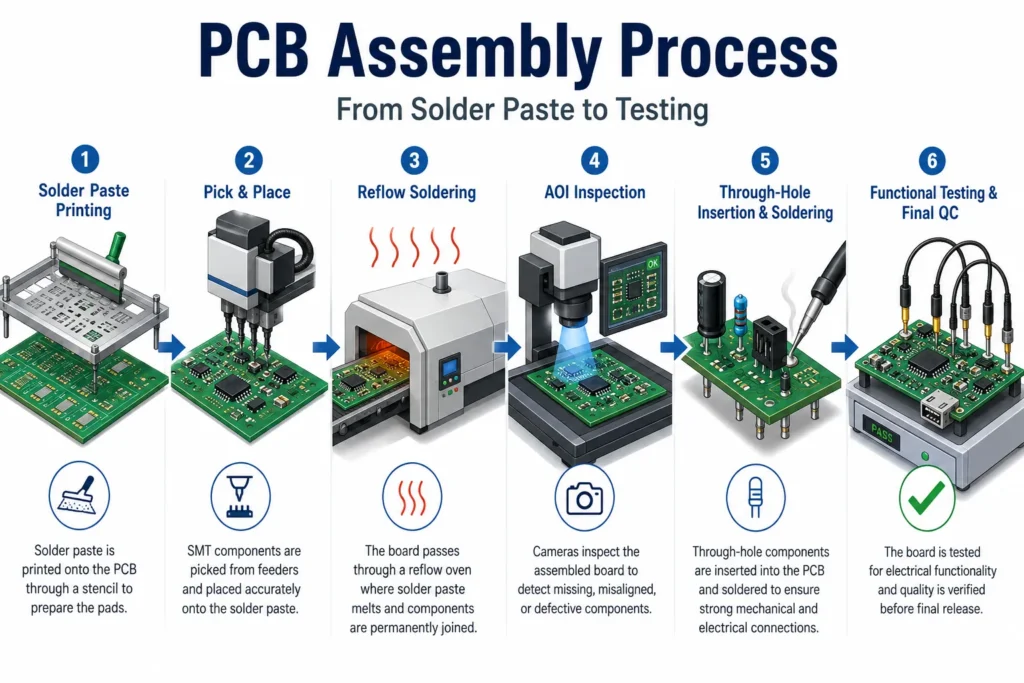
PCB assembly is the process of mounting and soldering electronic components onto a bare printed circuit board. The finished board is a printed circuit board assembly, or PCBA. A typical mixed-technology process has six main stages. They are printing, placement, reflow, optical inspection, optional through-hole assembly, and final testing.
This six-stage model supports planning and supplier discussions. It is not a fixed route. A simple surface-mount board may skip through-hole assembly. Another product may add X-ray, programming, cleaning, coating, or custom functional testing.
What Is the PCB Assembly Process?
A PCB is the unpopulated board that carries copper connections. It does not become a PCBA until components are mounted and joined to its pads or plated holes. PCB fabrication and PCB assembly are therefore different manufacturing operations.
Assembly planning starts before the line runs. The manufacturer needs a released BOM, centroid data, assembly drawings, and the correct PCB revision. It may also need programming files, test instructions, and packaging requirements. Every file should use one revision.
The route depends on component packages and board construction. Surface-mount devices (SMDs) normally use printing, placement, and reflow. Through-hole parts may follow and use wave, selective, pin-in-paste, or hand soldering. Choose inspection and testing for the product risk and agreed coverage.
Customers evaluating PCB assembly services should confirm the exact supply model, process route, inspection coverage, acceptance criteria, records, and deliverables before production.
PCB Assembly Process at a Glance
- Solder paste printing: A stencil deposits controlled amounts of paste on surface-mount pads.
- Pick and place: Placement equipment positions SMDs from feeders, trays, or tubes onto the printed paste.
- Reflow soldering: A controlled thermal profile activates the flux, melts the alloy, forms joints, and cools the assembly.
- AOI inspection: Cameras and programmed criteria check visible placement and soldering conditions.
- Through-hole assembly: Required leaded parts are inserted and soldered with a suitable process.
- Testing and final QC: Agreed inspections and electrical tests verify workmanship and required board behavior.
Double-sided or mixed-technology boards may repeat or reorder stages. The process engineer should define the traveler for the released assembly.
Solder Paste Printing
The surface-mount technology (SMT) assembly process usually begins with stencil printing. The stencil is aligned to the PCB. A squeegee moves solder paste across its surface. Paste passes through selected apertures and remains on the pads when the stencil separates from the board.
Paste volume must match the pad, package, stencil thickness, and aperture design. Too much paste can increase bridging or solder-ball risk. Too little can cause weak or open joints. Poor release, stencil contamination, inadequate board support, or alignment error can make deposits inconsistent.
Three-dimensional solder paste inspection, or 3D SPI, can measure deposit height, area, volume, and position before placement. Two-dimensional SPI provides more limited data. This helps detect print drift before components and reflow add more cost. Indium Corporation explains how transfer efficiency and SPI data help engineers evaluate print consistency.
A good print is not defined by one generic number. The acceptable window depends on the solder paste, stencil, aperture geometry, pad design, and package. Storage, thawing, mixing, and time on the stencil should follow the selected paste supplier’s instructions.
Pick and Place
After printing, a placement machine collects surface-mount components and positions them on the solder paste. Tape feeders are common for resistors, capacitors, and many integrated circuits. Trays or tubes may hold larger or unusual packages.
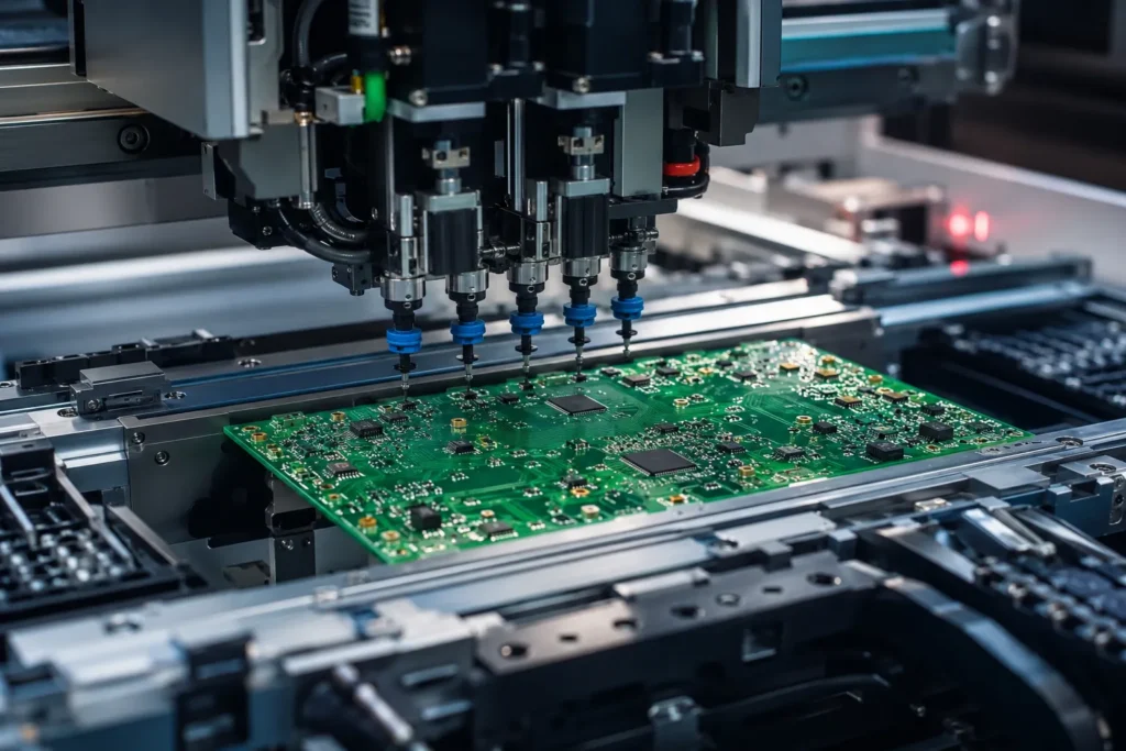
The machine program uses design coordinates, package data, rotation, and reference designators. PCB fiducials help align the program with the real board. Cameras can inspect component position on the nozzle. The system then corrects offsets before placement.
Accuracy depends on more than the machine specification. The nozzle, feeder setup, board support, component geometry, package coplanarity, and program data also matter. ASMPT describes how vision, component sensing, and offset correction support controlled placement.
Setup verification is essential. The part number, value, polarity, orientation, and feeder location must match the approved BOM and assembly data. A placement error can look small before reflow but create a short, open circuit, or difficult rework later.
Reflow Soldering
The placed board enters a reflow oven with controlled heating and cooling zones. The profile normally includes preheat, a thermal equalization region when required, time above the alloy liquidus, a peak, and cooling. During this cycle, flux prepares the surfaces and the solder alloy forms the joints.
The profile must fit the actual solder paste, components, PCB materials, and thermal mass. It should be measured on a representative assembly with thermocouples at critical locations. Oven air settings alone do not prove that every joint reached the required conditions.
There is no universal peak temperature or soak time for all boards. Excess heat can damage materials or exhaust flux. Too little heat can prevent wetting. Indium’s reflow optimization guidance shows why preheat, time above liquidus, peak temperature, and cooling must be considered together.
Common problems include bridging, tombstoning, poor wetting, voiding, and head-in-pillow. The oven profile may contribute, but printing, pad geometry, placement, oxidation, moisture, and package warpage can also be involved. Use process data to troubleshoot reflow soldering defects instead of changing every oven setting at once.
Automated Optical Inspection
Automated optical inspection uses cameras, lighting, and programmed criteria to examine the assembled board. Post-reflow AOI can flag missing or shifted parts, polarity errors, lifted leads, solder bridges, and other visible conditions. Some lines also use AOI after placement.
AOI is fast and repeatable, but it is not a complete test. It cannot prove that the circuit performs its intended function. It also cannot fully see solder joints hidden under BGA, QFN, or similar bottom-terminated packages. X-ray or another suitable method may be needed for those features.
OMRON describes AOI as a way to measure and classify visible solder joints. The program still needs approved criteria. Review false calls, then feed confirmed defects back to printing, placement, or reflow control.
For a deeper explanation of detectable defects, limits, and process feedback, see how AOI fits into PCB testing.
Through-Hole Component Insertion and Soldering
Not every PCBA uses through-hole components. When the design includes connectors, transformers, switches, or other leaded parts, they are inserted into plated holes. Insertion may be manual or automated. Polarity, seating height, lead condition, and mechanical support must be controlled.
Wave soldering can join many accessible through-hole leads in one pass. Selective soldering targets chosen areas and can protect nearby components. Hand soldering may suit prototypes, low quantities, or parts that need special handling. Pin-in-paste can reflow compatible through-hole parts with the SMT process.
The choice depends on layout, component heat limits, solder access, volume, and required control. Wave soldering is not best for every mixed assembly. ITW EAE notes that board design and component arrangement affect wave-solder process choices.
After soldering, visible joints are inspected against the agreed requirements. Hole fill, wetting, protrusion, bridging, contamination, and component damage may need review. Hidden or ambiguous conditions can require another method.
Functional Testing and Final Quality Control
Inspection and testing answer different questions. AOI checks visible workmanship. X-ray examines selected hidden joints. ICT or flying probe can check connections and selected component values. Functional circuit testing powers the PCBA and checks defined inputs, outputs, interfaces, or operating sequences.
A useful functional test needs customer-approved steps and pass/fail limits. It may also need firmware, a fixture, cables, loads, simulated signals, or a known test environment. NI describes functional test systems as configurable around the measurements and behavior a product must verify.
Functional testing is not automatically included in every standard PCB assembly order. The buyer and assembler should agree on method, coverage, sampling, fixture ownership, records, and failed-unit handling. Benlida’s guide to functional testing methods compares FCT with ICT, flying probe, AOI, X-ray, and boundary scan.
Final QC may also confirm revision, labels, serial numbers, workmanship, cleanliness, quantity, and packaging. J-STD-001 addresses soldering materials and process requirements. IPC-A-610 provides end-product acceptance criteria. The IPC document revision table lists current and historical revisions. Confirm the standard, revision, class, and customer-specific criteria before production.
What Changes the PCB Assembly Process?
- Component mix: Fine-pitch SMDs, BGAs, polarized parts, and through-hole devices need different handling and inspection.
- Board construction: Size, thickness, copper distribution, panel support, and thermal mass affect printing, placement, and heating.
- Assembly sides: A double-sided board may need a second print, placement, and reflow cycle.
- Order volume: Prototypes and stable production runs may justify different tooling, automation, and test fixtures.
- Risk and coverage: Hidden joints, safety functions, or costly failures can require wider inspection and test coverage.
- Special operations: Programming, cleaning, coating, depaneling, box build, and packaging add controlled stages.
These factors also affect schedule and price. Components, tooling, program preparation, first-article review, and test development may take longer than the line cycle. Ask for a scope-based quotation instead of assuming one fixed assembly time.
Files to Provide for PCB Assembly
A complete, revision-controlled data package reduces questions and setup risk. Provide the items that apply to your project:
- Gerber or ODB++ data, NC Drill files, and the approved bare-board specification.
- A BOM with manufacturer part numbers, quantities, reference designators, and approved alternatives.
- Pick-and-place or centroid data with X-Y coordinates, rotation, side, and reference designators.
- Assembly drawings that show polarity, special placement, do-not-install items, and mechanical details.
- Firmware files, revision, programming interface, and verification method when programming is required.
- Test procedures with operating conditions, measurable limits, sampling, records, and failure handling.
- Quantity, revision, supply model, labeling, final assembly, packaging, and target schedule.
Use one revision across every file. If a document replaces an earlier version, identify the change clearly. The assembler should resolve conflicts before components are loaded or boards enter production.
PCB Assembly Process FAQ
How long does the PCB assembly process take?
There is no universal duration. Component availability, board complexity, quantity, stencil and program preparation, first-article approval, inspection, and test development all affect the schedule. A simple repeat build can move faster than a new mixed-technology assembly with custom fixtures. Request a schedule for the released revision and agreed scope.
What is the difference between SMT and through-hole assembly?
SMT mounts components on PCB surface pads, usually with solder paste and reflow. Through-hole assembly inserts leads into plated holes. Those joints may use wave, selective, pin-in-paste, or hand soldering. Many PCBAs combine both methods because component and mechanical needs differ.
What happens during AOI inspection?
AOI captures images of the assembly and compares measured features with programmed criteria. It can flag visible placement, polarity, lead, and solder conditions. An operator or engineer reviews calls and traces confirmed defects to the process. AOI does not see every hidden joint and does not prove electrical function.
Is functional testing included in standard PCB assembly?
Not necessarily. Functional testing needs product-specific operating steps, limits, interfaces, and often a fixture or firmware. It should be listed in the quotation and production documents. Define coverage, sampling, result records, and the action for failed boards before the build starts.
Prepare Your PCB Assembly RFQ
A clear RFQ lets the supplier quote the real process instead of making assumptions. Send the current PCB files, BOM, centroid data, assembly drawings, quantity, revision, component-supply preference, and required inspection or test plan. Add firmware, fixtures, final assembly, labeling, and packaging instructions when they apply.
and ask for a review of the file package, process route, inspection coverage, test scope, records, and deliverables.

