Heavy Copper PCB Design — Thickness, Thermal Rules & Applications
Heavy copper PCB design commonly uses 3 oz/ft², or about 105 µm, on at least one layer. This is a common industry convention, not a universal standards definition. Extra copper can lower resistance and provide more conductor area for high current. It can also spread heat across a wider region. However, copper weight alone does not make a power path safe. Trace width, temperature rise, layer position, planes, vias, terminals, and cooling all matter.
The best design starts with electrical and thermal requirements. It then selects the lightest copper weight that meets those needs with practical geometry. Early fabrication review is essential. Thick copper changes etching, spacing, lamination, drilling, solder mask, and cost.
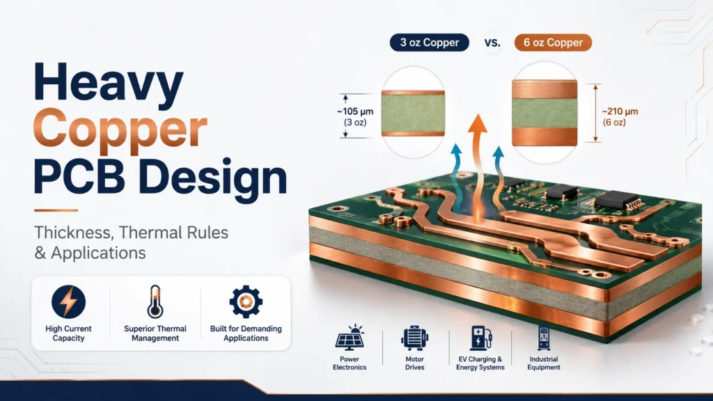
What Is a Heavy Copper PCB?
A heavy copper PCB has one or more layers with much thicker copper than a typical 1 oz design. Many suppliers use 3 oz as the starting point for the term “heavy copper.” Other suppliers may group 2 oz with high-current boards. The purchase drawing should therefore state the required copper for every layer. Do not rely on the label alone.
Copper weight means mass per unit area. The IPC-2152 current-carrying guide defines it in ounces per square foot or another mass-per-area unit. Designers often convert that value into nominal thickness. One ounce per square foot is about 35 µm, or 1.4 mil.
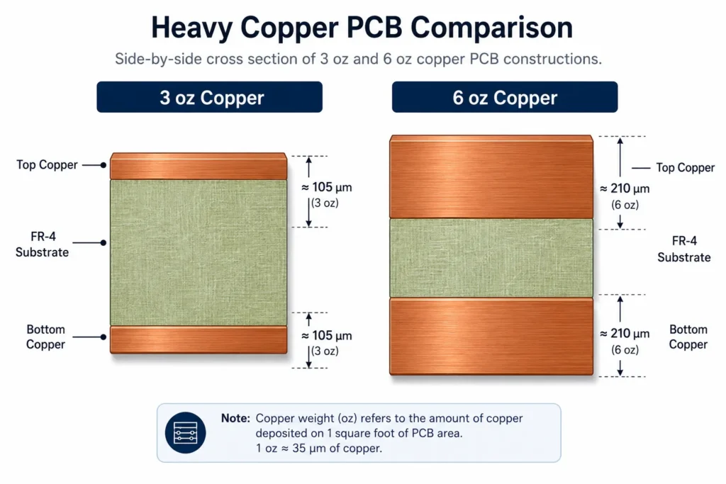
This conversion is useful for planning, but it is not a finished-board tolerance. Outer layers may combine base foil and plated copper. Inner layers usually follow a different process. Ask whether a quotation refers to starting foil, finished copper, or a minimum finished value.
Heavy copper does not remove voltage drop, heat generation, or current crowding. Those effects often appear at narrow necks, pads, vias, connectors, and fuse-like sections.
Copper Weight Options and When to Use Each
The table below is a planning guide. It does not assign a fixed current rating to any copper weight. Actual capacity depends on the complete conductor and its thermal environment.
| Copper weight | Approximate nominal thickness | Planning role | Design question |
|---|---|---|---|
| 1 oz | 35 µm / 1.4 mil | Common baseline for signals and moderate power | Can added width or a plane meet the load? |
| 2 oz | 70 µm / 2.8 mil | Higher-current rails with manageable feature sizes | Does 2 oz avoid the process impact of heavier copper? |
| 3 oz | 105 µm / 4.1 mil | Common entry point for heavy copper designs | What trace and spacing rules apply? |
| 4 oz | 140 µm / 5.5 mil | Power distribution with more conductor area | Can the stack-up fill around the copper? |
| 6 oz | 210 µm / 8.3 mil | Specialized high-current traces and planes | Are pads, holes, and solder mask manufacturable? |
| 8 oz | 280 µm / 11.0 mil | Very heavy power paths with larger geometry | Are etch shape and copper balance controlled? |
| 10–12 oz | 350–420 µm / 13.8–16.5 mil | Highly specialized power structures | Has the fabricator approved the layer construction? |
| 20 oz | 700 µm / 27.6 mil | Exceptional designs that need early process review | Would a busbar, metal insert, or another architecture work better? |
Do not select 20 oz simply because it offers more copper. Very thick copper can force wider features and larger clearances. It may also increase board thickness and restrict the stack-up. Compare heavy copper with parallel layers, bonded busbars, metal inserts, or another power-distribution method when appropriate.
How to Calculate Heavy Copper Trace Width
Trace width starts with continuous or RMS current, not copper weight. Define the maximum ambient temperature and the allowed conductor temperature rise. Then use finished copper thickness and layer position to estimate the required cross-sectional area.
A legacy chart-fit equation is widely used for a first estimate:
I = k × ΔT0.44 × A0.725
In this equation, I is current in amperes. ΔT is the permitted rise above ambient in degrees Celsius. A is the conductor cross-sectional area in square mils. The traditional coefficient is 0.048 for an external trace and 0.024 for an internal trace.
Rearrange the equation to estimate area:
A = [I ÷ (k × ΔT0.44)]1/0.725
Trace width in mils is then area divided by finished copper thickness in mils. A Texas Instruments high-current reference design shows this older relation in use. Treat the result as a screening value, not a released design rule.
IPC-2152 is the dedicated IPC guide for finished conductor size, current, and acceptable temperature rise. Its scope also covers board thickness, copper planes, layer environment, vias, and material effects. The current IPC document revision table lists IPC-2152 as no longer maintained and IPC-2221 at Revision C. Confirm the governing standard and method for each project.
A sound high current PCB design check should cover these items:
- Use worst-case continuous or RMS current, plus a separate transient and fault review.
- Check resistance, voltage drop, and power loss over the full path length.
- Model outer and inner layers with their actual nearby planes and cooling conditions.
- Review neck-downs, pads, thermal reliefs, slots, and current-sharing points.
- Calculate via barrels and connectors separately. Do not assume equal sharing without evidence.
- Apply design margin, then verify a representative prototype under worst-case conditions.
Thermal Management in Heavy Copper PCB Design
Heavy copper spreads heat, but it does not make heat disappear. Joule loss still follows I²R. Hot components can also inject heat into the same planes that carry current. The thermal plan should include the board, components, enclosure, airflow, interfaces, and duty cycle.
Use wide, direct paths and avoid abrupt reductions in width. Rounded or gradual transitions reduce current concentration near corners and pad entries. Large copper pours can spread current and heat.
Vias can move current or heat between layers. Their plating, finished hole size, count, spacing, and connection geometry control performance. A via array is not one solid conductor. Review via design for power and thermal paths before relying on parallel vias.
Thermal reliefs create another trade-off. They improve solderability by limiting heat flow into a plane. They also reduce conductor area at the pad. High-current terminals may need a different connection strategy. Assembly capability and serviceability still matter.
Measure temperature at risk locations such as neck-downs, terminals, switching devices, and enclosed hot zones. Validate at maximum ambient, load, and realistic airflow.
Where Heavy Copper PCBs Are Used
Heavy copper is useful when a board must route substantial current, spread heat, or combine control and power functions. Common candidates include converters, inverters, motor drives, power supplies, battery distribution, charging equipment, protection circuits, and industrial power controls.
Automotive electronics may also use heavy copper in power distribution, motor control, or charging systems. The construction alone does not make a board automotive-certified. Qualification, materials, documentation, and acceptance requirements must match the product program.
Industrial designs often combine noisy power switching with sensitive control signals. Layer planning, return paths, isolation, and thermal placement remain important. Benlida’s page on heavy copper PCBs for industrial control applications provides application context. It does not replace project-specific electrical and safety analysis.
Manufacturing Considerations for Heavy Copper
Thicker copper takes longer to etch. The conductor sidewalls may not remain perfectly vertical. Narrow traces and spaces that work with lighter copper may not transfer to a heavy copper process. Obtain approved production rules before routing the final layout.
Large thickness steps also affect lamination. Resin must fill around copper features without leaving weak or empty regions. Copper distribution should be balanced where possible. The stack-up must account for dielectric thickness, pressed thickness, and overall board tolerance. Use a documented PCB stack-up design instead of a simple layer count.
Pads, drilled holes, annular rings, and solder mask dams need extra attention. IPC-4562B covers procurement requirements for metal foil used in printed boards. The board drawing should state the agreed foil type, thickness, and finished requirements.
Send the fabricator a layer-by-layer copper table. Include the target finished thickness, minimum allowed thickness, board thickness, material system, current, voltage, temperature limits, and required tests. Mark critical power paths and unusual structures. Resolve differences between the schematic, layout, stack-up, and fabrication drawing before release.
For production planning, discuss heavy copper PCB manufacturing before freezing trace geometry. A separate PCB engineering consultation and DFM review can identify fabrication questions. Final electrical, thermal, safety, and compliance approval remains the customer’s design responsibility unless a contract states otherwise.
Heavy Copper PCB Design FAQ
What copper weight is considered heavy copper?
Many suppliers use 3 oz/ft², or about 105 µm, on one or more layers as the starting point. This is an industry convention, not a universal cut-off. State the required copper for each layer and define whether it is starting foil, finished copper, or a minimum finished value.
How is trace width calculated for a high-current PCB?
Start with continuous or RMS current, allowable temperature rise, layer position, and finished copper thickness. A legacy empirical equation can provide a first estimate. Then check voltage drop, planes, vias, neck-downs, cooling, and transient loads. Use an agreed IPC-2152-based method, simulation, and prototype testing for final validation.
What applications require a heavy copper PCB?
No application automatically requires heavy copper. It is a candidate for power conversion, motor drives, battery distribution, charging, protection, and industrial control. Select it when current, heat, voltage drop, space, reliability, and manufacturing studies support the choice.
Does a heavy copper PCB cost more to manufacture?
It often does, but there is no fixed premium. Cost depends on copper weight, layer count, board size, feature geometry, material, lamination, drilling, finish, quantity, testing, and process yield. Early DFM review can prevent unnecessary copper or a stack-up that is difficult to build.
Prepare a Heavy Copper PCB RFQ
Provide Gerber or ODB++, NC Drill files, a fabrication drawing, and an approved stack-up. Add the copper requirement for every layer, material, board thickness, surface finish, quantity, and revision. Include continuous and peak current, ambient conditions, allowed temperature rise, voltage-drop limit, and test requirements when available.
and send the current design package for manufacturability review. Ask the team to confirm copper definitions, trace and spacing rules, stack-up, vias, finished tolerances, tests, lead time, and quoted scope.

