

PCB Component Placement Guidelines for SMT
Why Component Placement Rules Matter for SMT
Good SMT component placement gives each part enough space for assembly, inspection, and repair. It also makes polarity clear, keeps handling areas accessible, and supports balanced heating during reflow. These decisions start in the PCB layout, before a placement machine touches the board.
The main checks are component spacing, orientation, board-edge clearance, thermal connections, and fine-pitch footprints. Set them around the actual packages and assembly process. A small resistor, a tall connector, and a BGA do not need identical clearance rules.
SMT placement accuracy also depends on equipment setup and board support. For example, ASMPT’s placement technologies use vision correction and support features to control component positioning. Good layout supports these processes, but it cannot compensate for incorrect placement data.
For the wider manufacturing sequence, see our PCB assembly process step by step. This guide focuses on the layout decisions that make that process easier to execute.
Minimum Spacing Between Components
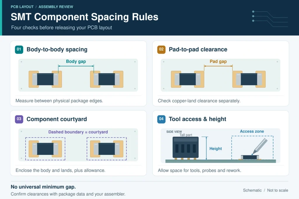
There is no single minimum spacing that suits every SMT component. Start with the package documentation and the assembler’s clearance rules. Then check access for placement tools, inspection, testing, and any planned rework.
Be clear about what the dimension measures. Body-to-body spacing measures the gap between physical packages. Pad-to-pad clearance concerns copper lands. The component courtyard encloses the body and land pattern with an allowance around them. A passing copper-clearance check does not prove that neighboring parts are easy to assemble.
Use accurate package outlines and component heights in the layout. A tall connector beside a small IC may limit tool access even when their footprints do not overlap. Leave additional room where a test probe, connector latch, or repair tool must reach.
The table summarizes minimum review conditions. The dimensions must come from the selected components and agreed manufacturing process.
Placement Rule
| Rule | Minimum Requirement | Reason |
|---|---|---|
| Component spacing | Meet approved courtyard, electrical, and assembly clearances. | Prevents interference and preserves required access. |
| Polarized parts | Verify polarity or pin 1 and keep assembly data consistent. | Reduces orientation ambiguity. |
| Transport edges | Keep specified conveyor and clamping zones clear on both sides. | Allows the panel to move and remain supported. |
| Depanelization | Respect the keepout for the chosen separation method. | Limits tool interference and component strain. |
| Thermal connections | Review pad heating while preserving the device's required heat path. | Supports soldering and operating thermal performance. |
| Fine-pitch and BGA parts | Use package-specific footprints and reserve agreed inspection and rework access. | Supports accurate assembly and later defect evaluation. |
Record the agreed PCB component spacing rules in the design constraints. Review exceptions with the assembler before releasing files.
Orientation Consistency for Polarized Components
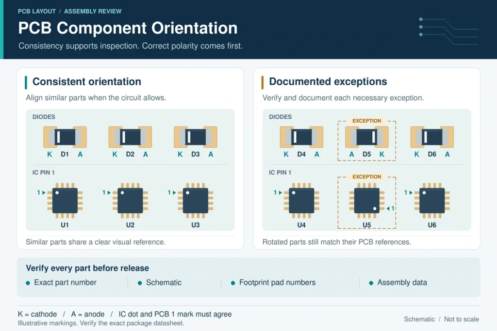
Keep similar polarized components facing the same direction where electrical and mechanical requirements allow. A consistent arrangement is easier to scan during assembly review. Necessary exceptions should be clear on the assembly drawing.
Correct polarity takes priority over visual alignment. Verify each diode’s anode and cathode, each polarized capacitor’s terminals, and each IC’s pin-1 position. Do not assume that a stripe always identifies the same terminal. NASA’s guidance on avoiding reversed capacitors highlights differences in marking conventions and the need to update drawings when parts change.
Check the schematic symbol, footprint pad numbering, and exact manufacturer’s part number together. A visually neat row can still contain an electrically reversed component.
Keep the BOM, assembly drawing, and pick-and-place file at the same revision. The placement file should identify reference designators, coordinates, board side, and rotation. Agree on coordinate and rotation conventions, especially for bottom-side parts. A zero-degree rotation in one library is not automatically the assembler’s expected orientation.
Make polarity marks readable without placing silkscreen over solderable pads. If the assembled part hides a mark, provide an unambiguous assembly drawing.
Placement Near Board Edges and Panel Rails
Check both the finished PCB outline and the assembly panel. Temporary panel rails can provide space for transport, clamping, and alignment features. Their usable area must match the equipment and tooling selected for the job.
Edge clearance can depend on component height and board side. Mycronic’s A40DX specifications illustrate this with different clearance conditions for bottom-side component heights. Treat such dimensions as machine-specific requirements, rather than universal PCB rules.
Ask which edges travel through the line and which areas must remain clear. Include underside components in this review. A connector overhanging the final board may still obstruct the conveyor while the board is inside its panel.
Panel rails also do not remove the need for a depanelization check. Routing, scoring, and breakaway tabs create different tool and mechanical constraints. Cadence’s component-to-edge clearance guidance explains why assembly access and board separation need separate attention.
Show the intended separation lines and keep nearby components outside the agreed affected area. Check alignment marks, tooling holes, and support locations before locking the panel drawing.
Thermal Relief and Large Component Placement
Thermal relief is a copper connection pattern around a pad. Narrow connections can reduce heat flow into a larger copper area during soldering. It is not a separate cooling feature placed beside a component.
For small two-terminal parts, review both ends together. Different pad connections, land shapes, or paste deposits can produce unequal soldering conditions. Murata’s chip capacitor mounting guidance explains how unbalanced soldering forces can lift one end of a part. This defect is called tombstoning.
Review pad symmetry, connected copper, paste volume, and placement position. Thermal relief may help some pad connections, but it is not a complete cure. The reflow profile and the component’s mounting instructions still matter.
Avoid applying thermal relief to every connection automatically. Some devices need a direct path into copper planes to remove heat during operation. For example, TI’s PowerPAD guidance calls for solid thermal-via connections to the planes. Follow the exact device requirements for exposed pads, thermal vias, and high-current paths.
Large components and dense copper areas can change how nearby joints heat. Review these locations during thermal profiling on a representative assembly. Oven settings alone do not establish the temperature reached at each joint. Also preserve access around tall parts for placement and inspection.
For troubleshooting after assembly, use our guide to SMT process defects and prevention.
Placement Rules for Fine-Pitch and BGA Components
Fine-pitch placement starts with the correct package footprint. Confirm the exact package variant, lead or ball pitch, and pin-1 or A1 orientation. Do not reuse a footprint simply because its body outline looks similar.
Plan escape routing before fixing a BGA’s position. The ball map, via structure, routing channels, and stackup must work together. TI’s nFBGA layout guidance illustrates these package-dependent planning decisions.
Review the copper lands, solder-mask openings, and stencil apertures as a set. Analog Devices’ BGA assembly guidance connects these features with paste deposition and rework requirements. Set dimensions from the actual package guidance and validated process.
Reserve space for the selected rework nozzle and nearby component heights. Keep agreed fiducial areas clear so the assembly equipment can locate the board or local placement region. Confirm whether local fiducials are needed with the assembler.
Plan inspection early. BGA joints sit beneath the package, so ordinary top-down visual inspection cannot examine the full joint array. X-ray can help evaluate hidden solder conditions. Electrical and functional testing address different questions and should follow the project’s test plan.
FAQ
What is the minimum spacing between SMT components?
There is no universal gap. Use the package footprint, courtyard, electrical clearance, and assembler’s access requirements. Include component height and planned rework. Confirm whether a quoted dimension measures package bodies, copper pads, or courtyard boundaries.
Why does component orientation consistency matter for assembly?
Consistent orientation makes similar parts easier to review and helps people notice exceptions. It supports inspection but does not prove correct polarity. Verify the exact part, pad numbering, and assembly data, even when all parts face the same direction.
Can components be placed close to panel edges?
Only when they remain outside the agreed transport, clamping, and separation keepouts. Check both board sides and component heights. A temporary rail may provide handling space, but the finished board’s separation line still needs its own review.
Does BGA placement require special layout considerations?
Yes. Check the ball map, orientation, land pattern, solder mask, stencil, and escape routing together. Allow for assembly alignment and rework tooling. Agree on how hidden joints and electrical function will be inspected and tested.
Optimizing Your Layout for SMT Placement?
Benlida reviews component spacing and orientation during DFM to reduce placement errors before production.
Explore our SMT assembly services. Request an SMT placement review. Send the PCB files, BOM, pick-and-place data, and assembly drawing with the same revision. Include panel constraints, component heights, and any inspection or rework requirements.