

PCB Copper Weight Selection Guide — Choosing the Right Oz Rating

What Is PCB Copper Weight?
PCB copper weight describes the mass of copper per unit area, usually in ounces per square foot, or oz/ft². One ounce corresponds to about 35 µm of nominal copper thickness. Copper weight affects trace resistance and heat spreading. It does not, by itself, define a safe current rating.
Choose copper thickness together with trace width, allowable temperature rise, voltage drop, and manufacturing limits. A wider 1 oz trace may meet your requirements without heavier copper. Where routing space is limited, thicker copper may be worth evaluating.
First, distinguish starting foil from finished copper. Eurocircuits’ copper-thickness guidance explains this difference. Outer layers commonly gain copper during plating, while cleaning and etching remove some copper. Conventional inner layers mainly depend on the starting foil; specialized via structures can use different processing.
Specify the required finished copper for each layer. State whether a value is nominal or a required minimum, and agree the tolerance and inspection method. Do not assume that a quote for “1 oz copper” guarantees 35 µm at every point.
Standard vs Heavy Copper Weight Options
Common starting points include 0.5 oz, 1 oz, and 2 oz. One-ounce copper is widely used for general routing. Two-ounce copper offers more cross-sectional area at the same width. Neither option is automatically suitable for every power net.
Heavy copper often means 3 oz or more on at least one layer. This is a commercial convention, not a universal boundary. NCAB’s heavy-copper overview also uses 3 oz as its starting point. Always specify actual thickness instead of relying on the label.
Nominal equivalents are approximately 70 µm for 2 oz, 105 µm for 3 oz, and 140 µm for 4 oz. These describe thickness, not the board’s total copper mass. They also do not establish a manufacturer’s available range.
You may need different copper weights on power and signal layers. Ask the fabricator to propose a suitable, balanced stackup before routing. Increasing every layer’s copper weight can create unnecessary layout and cost constraints.
Copper Weight and Current Capacity
Current creates resistive heat in a trace. At the same width, length, and temperature, thicker copper lowers resistance. The resulting temperature rise also depends on the surrounding board and how heat escapes.
IPC-2152 specifically addresses conductor sizing, current, and temperature rise. It considers factors such as board construction and copper planes. Agree the design method and applicable standard edition with your engineering team.
For a simple comparison, TI’s PCB layout guidance reproduces a legacy IPC-2221 trace-width equation. Rearranged for an external trace, it is:
I = 0.048 × ΔT0.44 × A0.725
Here, I is current in amperes, ΔT is temperature rise in °C, and A is conductor cross-sectional area in square mils. Area equals width multiplied by thickness. One mil is 0.0254 mm.
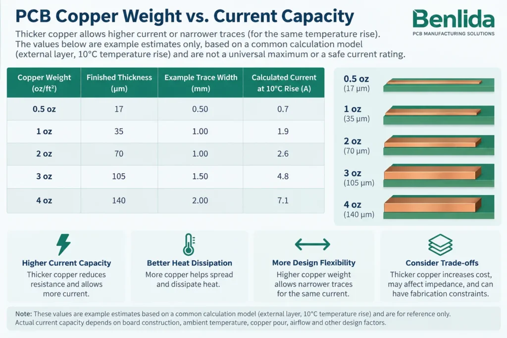
The following example fixes the external trace width at 1.0 mm and temperature rise at 10°C. It assumes the uniform copper thicknesses shown. Values are rounded calculations, not measurements, IPC-2152 results, or universal safe-current limits.
Copper Weight vs Current Capacity — Illustrative Legacy-Model Estimates
| Copper Weight / Assumed Thickness | Example Trace Width | Calculated Current at 10°C Rise |
|---|---|---|
| 1 oz / 35 µm | 1.0 mm, external | About 2.4 A |
| 2 oz / 70 µm | 1.0 mm, external | About 4.0 A |
| 3 oz / 105 µm | 1.0 mm, external | About 5.3 A |
| 4 oz / 140 µm | 1.0 mm, external | About 6.5 A |
Doubling thickness increases the calculated current by about 65% in this model, not 100%. The model does not explicitly resolve your enclosure, nearby heat sources, or cooling arrangement. Use it for comparison, then evaluate the actual assembly.
For steady DC, check continuous current. For changing current, use the full-waveform root-mean-square (RMS) current to assess resistive heating, not the average alone. Check peak current, pulse duration, and significant high-frequency effects separately. A 10°C rise allowance is a design input, not a universal requirement.
Trace Width Trade-Offs at Higher Copper Weights
Extra thickness can reduce the width needed for a target cross-sectional area. However, that electrical benefit does not mean finer manufacturing features become easier.
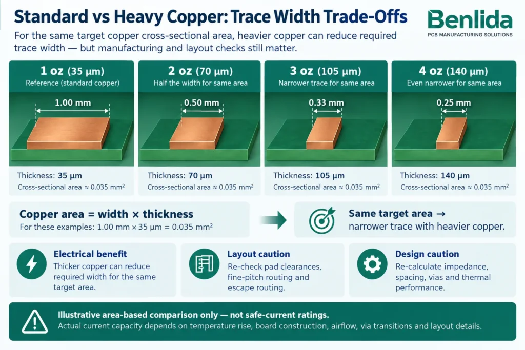
Thicker copper is harder to etch into tight traces and gaps. Epec’s copper-weight and spacing guidance explains why heavier copper needs greater etch compensation. Confirm the allowed finished line width and spacing for your selected copper and process.
Do not increase copper weight after routing without checking fine-pitch pads, gaps, and escape routing again. Where impedance matters, recalculate the stackup and trace geometry. Also confirm dielectric spacing and voltage-clearance requirements; heavier copper does not replace insulation.
Check the whole current path. A wide trace may narrow at a connector pad, fuse, or component lead. A plane may contain narrow bridges around cutouts. These local restrictions can matter more than the broad copper area nearby.
Review via barrels and layer transitions separately. Surface copper weight does not specify via-wall copper thickness. For more detailed fabrication considerations, use the heavy copper PCB design guide.
When to Choose Heavy Copper Over Standard
Consider heavy copper when the required current path cannot fit within the available routing area using lighter copper. It may also help when voltage drop or copper loss is too high. These conditions can arise in power converters, motor drives, and power-distribution boards.
Start by identifying the limiting requirement. Is the trace too hot, the voltage drop too large, or the route too wide? More copper is useful only if it addresses that problem.
- Define continuous current, current waveform, ambient conditions, and acceptable temperature rise.
- Estimate trace resistance, voltage drop, and loss using the expected finished geometry.
- Compare a wider route, thicker copper, additional current paths, or another suitable interconnect.
- Check layout and manufacturing feasibility, then validate the preferred option under the intended load.
Thicker copper can spread heat laterally, but heat still needs a path out of the assembly. TI’s PCB thermal-design guidance discusses copper planes alongside vias, heat sinks, and airflow. A heavier layer alone cannot guarantee component temperature.
The PCB thermal management design guide covers those wider choices. Test the finished assembly in its enclosure, including nearby heat sources and realistic cooling. A bare-board calculation cannot capture every operating condition.
Copper Weight and Manufacturing Cost Impact
Higher copper weight usually increases fabrication cost, but there is no universal surcharge. Material usage is only part of the difference. Etching, plating where required, and process control can also change.
Thicker copper features may require a different prepreg construction to fill the spaces between them during lamination. Solder-mask coverage and the finished surface profile also need review. Confirm the resulting board thickness before committing to enclosure dimensions.
For an assembled board, discuss the added thermal mass with the assembly supplier. Soldering profiles and thermal-relief connections may need attention. A bare-PCB price comparison can miss those assembly effects.
Compare quotes using the same quantities, board outline, stackup, finished copper requirements, acceptance criteria, and revision. Ask which design changes drive the price difference. Do not assume that moving from 1 oz to 2 oz doubles board cost.
Choose the lowest-complexity construction that meets the verified electrical, thermal, and reliability requirements. Document any proposed copper change and obtain engineering approval before releasing a revised manufacturing package.
FAQ
What copper weight is standard for most PCBs?
One-ounce copper is a common general-purpose choice, and 2 oz is also widely used. There is no single required value for every PCB. Check the copper specification by layer and confirm whether it means starting foil or finished thickness.
At what point is a board considered “heavy copper”?
The term often starts at 3 oz on at least one layer, but supplier definitions vary. Treat it as a descriptive category. State the actual finished thickness, tolerance, and layer locations in the fabrication requirements.
Does higher copper weight increase manufacturing cost?
Usually, yes. More copper and tighter process demands can increase cost. The difference depends on the complete board design and order quantity. Request comparable quotes rather than applying a fixed percentage.
How do I calculate trace width for a given copper weight?
Start with current, allowed temperature rise, layer position, and finished copper thickness. Use a documented conductor-sizing method, then check voltage drop and manufacturing limits. Include neck-downs, vias, and connectors. Verify performance on the actual assembly.
Not Sure Which Copper Weight Fits Your Design?
Send Benlida your Gerber or ODB++ files, drill data, stackup, and fabrication drawing. Specify finished copper by layer, trace dimensions, quantity, and revision. Include current waveforms, ambient conditions, allowable temperature rise, and voltage-drop limits.
Discuss your options through Benlida’s heavy copper PCB manufacturing service. Ask the team to confirm manufacturing feasibility and DFM scope. Agree separately whether electrical calculations or thermal analysis are included; a manufacturability review does not replace design validation.