

PCB Design for Testability — DFT Best Practices

What Is Design for Testability?
PCB design for testability, or DFT, means planning how an assembled board will be controlled, measured, and checked before its design is released. It may involve test pads, connectors, test modes, or boundary scan. The aim is to make specified faults easier to detect and locate without unnecessary production work.
DFT starts with a test plan, not a target number of pads. Decide which connections, component characteristics, and product functions need verification. Then give the chosen equipment access to them.
This article focuses on testing populated boards, or PCBAs. Bare-PCB electrical testing checks the unassembled board’s connections and isolation. It cannot verify installed components or firmware. The broader guide to PCB functional testing methods explains how assembly tests fit together.
The table summarizes common test approaches and their design implications. They can be combined; a flying-probe system may perform selected in-circuit or powered tests.
| Method | Access Required | Best For | Limitations |
|---|---|---|---|
| Fixture-based ICT | Probe targets, locating features, and board support. | Repeatable checks of selected connections and component characteristics. | Fixture investment; coverage depends on access, circuitry, and the test program. |
| Flying probe | Reachable contact targets and room for moving probes. | NPI, changing designs, and builds that do not justify a dedicated bed-of-nails fixture. | Probe movement affects cycle time; available tests depend on system configuration. |
| Boundary scan | Supported devices, a working scan chain, and controller access. | Selected digital interconnect checks where physical access is limited. | Not every pin or net is covered; analog and product behavior need additional checks. |
| Functional test | Power, interfaces, required loads, and defined test controls. | Checking specified board functions under defined conditions. | Coverage and fault isolation depend on the procedure and available measurements. |
Test Point Placement Rules
Useful test point placement on a PCB starts with electrical purpose. Identify required power and ground access, measurements, programming connections, and test controls. Do not add a pad to every net without checking whether it helps the test plan or harms circuit performance.
Agree these details with the test engineer and fixture supplier:
- Finished contact-pad dimensions, center-to-center spacing, and placement tolerances.
- Clearance from nearby components, including their height and probe approach direction.
- Access side, board-edge keepouts, clamp locations, and support points.
- Surface finish, solder-mask opening, and any coating or contamination concerns.
- Test-point names, net names, coordinates, and their common drawing revision.
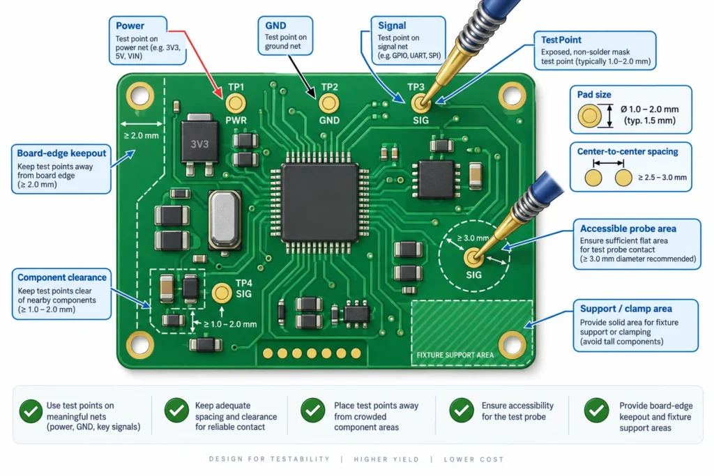
There is no universal minimum pad size. The contact target must suit the probe, fixture alignment, and manufacturing tolerances. A nominal copper diameter alone does not establish reliable contact.
INGUN’s test-probe guidance explains how tip shape, spring force, and surface condition affect contact. More force is not automatically better. Review possible pad damage and board bending, particularly around fragile components.
Keep designated exposed probe pads clear of solder mask and insulating coatings. If testing occurs after conformal coating, agree the access strategy in advance. Verify clearance on the populated assembly, not only the bare-board layout.
ICT Access and Bed-of-Nails Considerations
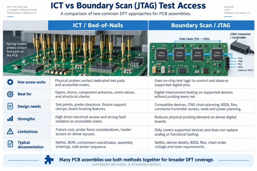
In-circuit testing, or ICT, checks selected components and connections through electrical access. Keysight’s ICT overview describes checks such as opens, shorts, and incorrect component values. The circuit and test program determine which faults can actually be detected.
A bed-of-nails fixture uses spring-loaded probes at fixed locations. It needs repeatable board positioning and enough support to handle the combined probe force. Leave space for locating features, supports, clamps, and tall parts on both sides.
Concentrating access on one side can simplify some fixtures, but it is not a universal rule. Confirm whether the tester supports the required access arrangement. Check panel rails and handling restrictions if boards will be tested before depanelization.
Provide schematics, a netlist, BOM, component coordinates, and assembly drawings for test development. Gerber files alone do not define component values, operating states, or pass/fail limits. Agree safe power sequencing and any unpowered checks before the board is energized.
ICT test access must also support diagnosis. A fixture that can reach many pads may still struggle to isolate a fault if parallel circuit paths interfere with measurements.
Boundary Scan (JTAG) Design Support
Boundary scan uses test logic inside supported devices to control and observe selected pins. The IEEE 1149.1 architecture provides a test access port, or TAP. It can support digital interconnect checks without placing a physical probe on every covered connection.
A JTAG debug connector does not prove boundary-scan readiness. Confirm the exact device, package, supported instructions, and test-mode requirements. Some pins or interfaces may not be testable through the chosen scan implementation.
Obtain the matching Boundary-Scan Description Language, or BSDL, files. TI’s explanation of BSDL shows why these device descriptions and the board netlist are key inputs for developing structural tests.
Include these checks in boundary scan design:
- Route clock, mode-control, and serial-data signals according to device and controller requirements.
- Verify chain order, voltage compatibility, power availability, and reset behavior.
- Provide controller access, ground references, and ways to diagnose a broken chain.
- Plan bypass connections where optional, unpopulated devices would otherwise break the chain.
XJTAG’s DFT guidelines discuss these chain-design constraints and complementary testing. Retain access for measurements that ordinary boundary scan cannot provide. Digital connectivity checks do not automatically verify analog accuracy, power quality, or full-speed product operation.
DFT for High-Density and Fine-Pitch Boards
Dense layouts need a selective access plan. Prioritize critical rails, control signals, and measurements that other methods cannot provide. Review whether boundary scan can cover suitable digital nets before adding difficult-to-reach pads.
Do not solve an access problem by creating a signal-integrity problem. A branch leading to a test pad can form an unwanted stub. TI’s M-LVDS layout discussion specifically warns about test-point stubs on differential lines. Follow the relevant interface guidance and evaluate any added pad, via, or branch.
Smaller probes may help, but they do not remove clearance, alignment, or support requirements. Seica’s flying-probe overview illustrates systems that combine different test capabilities. Confirm the actual platform and program; moving probes do not guarantee access to every fine-pitch connection.
Use inspection to address different risks. AOI checks visible assembly features, while X-ray inspection for hidden joints can examine selected solder structures beneath packages. Neither image-based method proves circuit operation. Likewise, an electrical pass does not establish the physical condition or long-term reliability of every solder joint.
How DFT Can Reduce Functional Test Cost
DFT can reduce avoidable test development and troubleshooting work. For example, a board that fails to boot is easier to investigate when engineers can measure its supply rails and control reset. Without suitable access, diagnosis may require temporary wiring or a revised fixture.
Plan test commands, repeatable startup conditions, and useful diagnostic outputs with the firmware team. Define loads, interface connections, measurement limits, and recovery steps. A simple pass/fail light may be insufficient for locating a production fault.
Compare total test cost at the expected build quantity. Include fixture design, programming, validation, cycle time, maintenance, and fault diagnosis. A dedicated fixture may suit a stable production design. Flying probe can avoid that fixture investment, but board holding, programming, and test time still have costs.
Before layout release, prepare a controlled test handoff package:
- Schematic, netlist, BOM, layout data, and assembly drawings with matching revisions.
- Test-point coordinates, fixture restrictions, and any BSDL files.
- Required firmware, test modes, interfaces, loads, and power sequence.
- Fault-coverage targets, pass/fail limits, known gaps, and required records.
These DFT best practices can simplify testing, but savings depend on the product and process. They do not guarantee complete fault detection or replace product validation.
FAQ
What is the minimum test point size for ICT?
There is no single minimum for all ICT systems. Pad size depends on probe geometry, alignment, surface condition, and manufacturing tolerances. Ask the test and fixture teams for approved finished-pad dimensions, spacing, and clearances before routing. Do not use another supplier’s minimum as your production rule.
Does boundary scan replace the need for test points?
No. It can reduce physical access needs for supported digital connections. Power measurements, analog checks, programming, debug, or scan-chain diagnosis may still require physical access. Confirm coverage using the actual devices, BSDL files, netlist, and test tools rather than assuming every pin is covered.
How early should DFT be considered in the design process?
Start during system architecture and schematic design. Choose the test strategy before component placement and routing constrain access. Review it again before layout release and validate it during prototypes. Update the test plan whenever hardware, firmware, or production requirements change.
Can Benlida review my layout for testability before manufacturing?
You can request a project-specific review from Benlida. Share the layout, schematic, BOM, and test requirements. When discussing functional testing services, confirm whether test-point review, ICT access assessment, fixture development, or boundary-scan support is included. These activities should not be assumed from a general DFM review.
Designing for Easier Testing?
Send Benlida your design files, proposed test plan, build quantity, and known access constraints before layout release. Ask engineering which review and test-development activities can be supported. Agree the scope, required customer inputs, and acceptance criteria before production begins.