Rigid-Flex PCB Design Guide — Stack-Up Rules, Materials & Common Mistakes
A rigid-flex PCB combines rigid FR-4 sections and flexible polyimide circuits in one connected board.
Reliable rigid-flex PCB design depends on a balanced stack-up, suitable materials, controlled bend zones, and vias placed only in rigid areas.
These rules reduce mechanical stress, improve reliability, and simplify assembly.
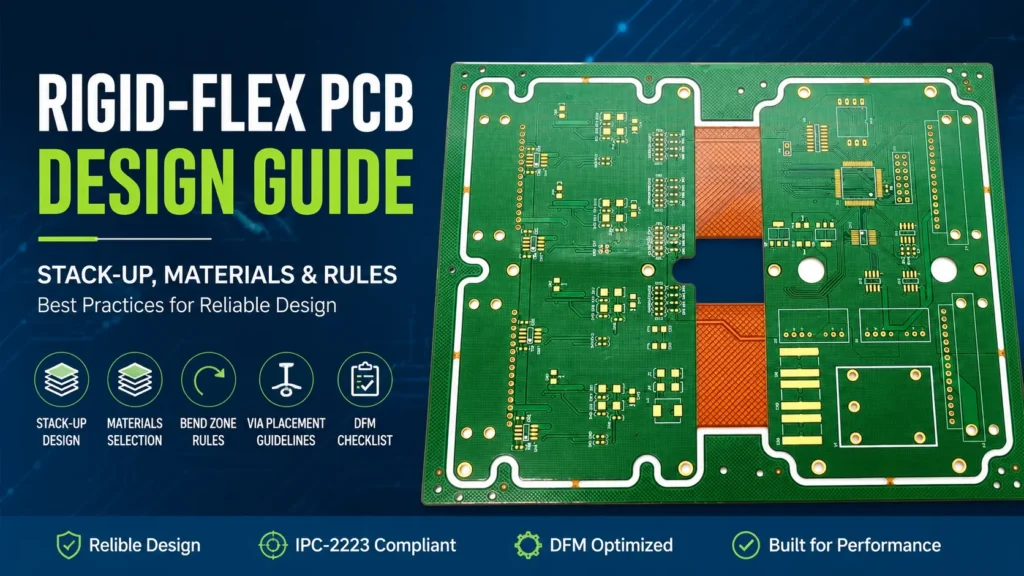
A rigid-flex PCB combines rigid board sections with flexible circuit sections in one connected structure. This can reduce connectors, save space, and improve assembly reliability. However, the design must control stress in the flex area. It must also match the fabrication process from the start.
This guide explains the main rigid-flex PCB design rules in simple terms. You will learn how to plan the stack-up, select materials, design bend zones, place vias, and prepare files for a DFM review.
What Is a Rigid-Flex PCB?
A rigid-flex PCB is a circuit board that includes both rigid and flexible areas. The rigid areas hold components, connectors, and other parts. The flexible areas bend or fold to connect the rigid sections.
The flexible layers usually continue through the rigid sections. This creates one integrated circuit instead of several separate boards joined by cables. The result can be smaller and lighter. It can also reduce the number of connectors and solder joints.
Rigid-Flex PCB vs. FPC vs. Rigid PCB
| Feature | Rigid-Flex PCB | FPC | Rigid PCB |
|---|---|---|---|
| Structure | Rigid and flexible sections integrated into one board | Mainly flexible material, sometimes with local stiffeners | Fully rigid laminate structure |
| Bending | Bends only in defined flex zones | Can bend across selected flexible areas | Not designed to bend |
| Component Placement | Components are mainly mounted on rigid sections | Components usually need stiffened or supported areas | Components are mounted directly on the rigid board |
| Interconnections | Can reduce cables and board-to-board connectors | Often used as a lightweight flexible interconnect | Separate boards usually require cables or connectors |
| Typical Applications | Compact 3D assemblies and high-reliability electronics | Lightweight devices and space-limited connections | Standard flat electronic assemblies |
| Design Complexity | High | Medium | Low to medium |
Rigid-flex PCB is usually selected when a product needs both mechanical support and controlled flexibility. FPC is better for lightweight interconnections, while rigid PCB remains suitable for standard flat assemblies.
Rigid-Flex PCB Stack-Up Design
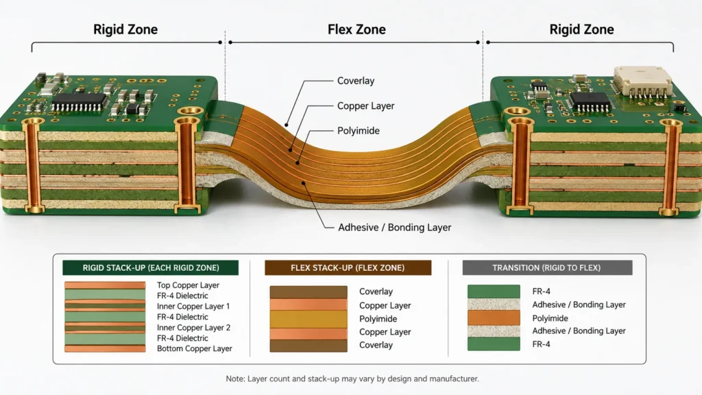
The stack-up is the foundation of rigid flex PCB design. It defines the number of copper layers, dielectric layers, coverlay layers, and bonding materials. It also controls the total thickness of the flex area.
The stack-up is an electrical, mechanical, and manufacturing decision. Ask the fabricator to review it before routing begins.
Separate the Rigid and Flex Requirements
Start by marking every rigid zone, flex zone, and transition zone in the mechanical drawing. Define which areas will carry components. Define which areas will bend once during assembly and which areas will move many times in service.
Static and dynamic bends need different rules. Dynamic areas usually need fewer copper layers, thinner materials, and a larger bend radius.
Plan Layer Transitions Early
The flex layers may pass through the rigid section as inner layers. The rigid section then adds FR-4, prepreg, and outer copper. The transition from thick rigid material to thin flex material creates a stress point.
Keep the transition shape smooth. Avoid sharp corners in the board outline. Use a gradual radius where possible. Do not place pads, vias, or narrow traces directly at the rigid-to-flex boundary.
Keep the Flex Stack Symmetrical When Possible
A balanced flex stack bends more evenly. Uneven copper or dielectric thickness can move the neutral bend area away from the center. This can increase strain on one copper layer.
Keep copper distribution balanced when the electrical design allows it. Ask the fabricator to check lamination and registration risks.
Use Coverlay in Flexible Areas
Flexible areas usually use coverlay instead of standard rigid-board solder mask. Coverlay protects the copper and provides insulation. It also moves with the flex circuit.
Confirm coverlay opening clearance and alignment tolerance with the manufacturer.
Material Selection for Rigid-Flex PCB
Rigid flex PCB materials must work together as one structure. The main choices include polyimide film, FR-4, copper foil, coverlay, bonding film, and adhesive systems. Each choice changes flexibility, thickness, cost, thermal performance, and reliability.
Polyimide for the Flex Core
Polyimide is widely used as the dielectric in flexible circuits. It offers good heat resistance, electrical insulation, and mechanical flexibility. Material suppliers offer different polyimide thicknesses and laminate constructions.
Thinner polyimide can improve flexibility, but it is harder to process. Choose thickness based on layer count, impedance, and bend needs.
FR-4 for the Rigid Sections
FR-4 is commonly used in the rigid areas. It gives the board mechanical support and provides familiar processing for component assembly. High-Tg or other special FR-4 grades may be needed for higher temperatures or demanding reliability targets.
Adhesive and Adhesiveless Flex Laminates
Adhesive-based laminates use an adhesive layer between copper and polyimide. They are common and cost-effective for many products. Adhesiveless laminates remove that extra adhesive layer. This can reduce flex thickness and may improve dimensional and thermal performance.
Review bend cycles, temperature, copper thickness, impedance, chemical exposure, and assembly conditions before choosing a laminate.
Rolled-Annealed and Electrodeposited Copper
Rolled-annealed copper is often selected for areas that must bend many times. Its grain structure can support repeated flexing better than standard electrodeposited copper in many applications. Electrodeposited copper is still suitable for many static-flex designs and can offer cost or processing benefits.
Confirm copper type and thickness with the fabricator because both affect bend life.
DuPont publishes information on polyimide films and flexible circuit laminate systems. These references can help designers understand the range of available laminate, coverlay, and bonding options: DuPont flexible circuit laminates.
Bend Zone Design Rules
The bend zone is the most sensitive part of a rigid-flex PCB. Copper in this area is exposed to tension and compression. Small layout choices can have a large effect on reliability.
Set the Bend Radius from the Real Application
There is no single bend radius that fits every rigid-flex design. The correct value depends on total flex thickness, copper thickness, layer count, bend angle, and the number of bend cycles.
Use a larger radius whenever space allows. A larger bend radius lowers mechanical strain. For detailed calculations and design examples, see Benlida’s FPC bend radius rules.
Route Traces Across the Bend
Route traces as close as possible to perpendicular to the bend line. This helps each trace cross the bend over a shorter and more controlled path. Avoid running long traces parallel to the bend axis.
Keep Trace Width Consistent
Sudden width changes can concentrate stress. Keep trace width consistent through the bend zone. Use smooth curves instead of sharp corners. Add teardrop transitions where traces meet pads when the design rules allow it.
Avoid Solid Copper in the Bend Area
Large solid copper pours make the flex area stiffer. They can also create uneven bending. Remove unnecessary copper from the bend zone. If shielding or a reference plane is required, discuss a hatched pattern with the fabricator.
Keep Components and Pads Out of the Bend Zone
Components should normally stay on rigid sections. Pads and solder joints do not tolerate repeated bending well. Leave a clear keep-out area between the bend zone and the nearest component pad.
Add Strain Relief at Transitions
The rigid-to-flex edge can act as a hinge. Rounded transition corners, suitable coverlay extension, and controlled stiffener geometry can reduce local stress. The exact strain-relief method depends on the stack-up and enclosure.
IPC identifies IPC-2223 as the sectional design standard for flexible and rigid-flexible printed boards. Designers should use the latest released revision and confirm its current status on the IPC board design standards page.
Via Placement Rules in Rigid-Flex PCB
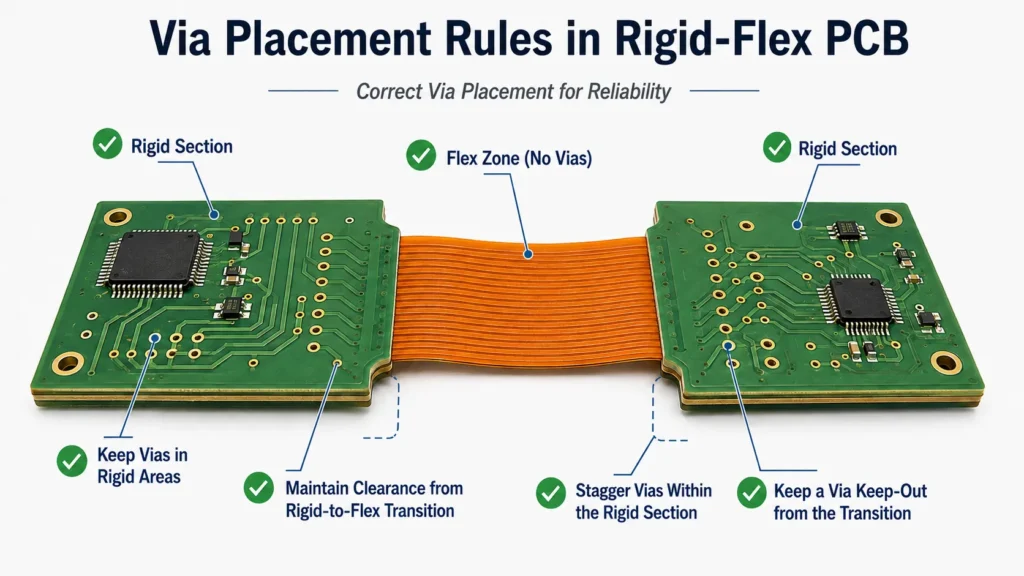
Vias are rigid plated structures. They should not be placed in an area that must bend. Bending near a via can stress the barrel, pad, and surrounding dielectric.
Keep Vias Inside the Rigid Zone
Place through holes, blind vias, buried vias, and microvias in rigid sections whenever possible. Define a via keep-out distance from the rigid-to-flex transition. The required distance depends on the stack-up and fabrication capability.
Do Not Create a Straight Stress Line
A straight row of vias near a transition can form a weak line. Stagger vias when the electrical layout allows it. Avoid dense via fields near the bend zone.
Check Annular Rings and Pad Sizes
Rigid-flex lamination can make registration more difficult than a standard rigid PCB. Small annular rings may leave less process margin. Use realistic drill, pad, and registration tolerances from the selected manufacturer.
Common Rigid-Flex PCB Design Mistakes
Most rigid-flex PCB failures begin with stack-up, bend-zone, or transition-area decisions. The following table explains the most common problems and how to prevent them.
| Mistake | Why It Is a Problem | Recommended Fix |
|---|---|---|
| Adding a flex section to a rigid PCB stack-up later | The flex area may become too thick or stiff, which increases stress at the transition. | Plan the complete rigid-flex stack-up before routing begins. |
| Using unsuitable copper thickness in the flex zone | Thick or unbalanced copper can reduce flexibility and increase mechanical strain. | Select copper thickness based on bend cycles, layer count, and flex requirements. |
| Defining the bend radius after routing | The final bend may conflict with traces, vias, component keep-outs, or the enclosure. | Define the bend line, bend angle, and bend radius before detailed routing. |
| Placing vias, pads, or components in the flex zone | Rigid features can crack, delaminate, or create concentrated stress during bending. | Keep these features inside rigid sections and define a transition keep-out area. |
| Using excessive solid copper in the bend area | Large copper areas make the flex zone stiffer and cause uneven bending. | Remove unnecessary copper and use a balanced or hatched pattern when required. |
| Using sharp corners at the rigid-to-flex transition | Sharp corners concentrate mechanical stress and increase the risk of cracking. | Use rounded contours, smooth width changes, and suitable strain relief. |
| Ignoring copper type or grain direction | An unsuitable copper construction can reduce the service life of repeated bends. | Confirm copper type and bend direction with the rigid-flex PCB manufacturer. |
| Skipping an early DFM review | Manufacturing limits may be discovered after routing, causing redesign and delays. | Request a DFM review before releasing the final fabrication files. |
Benlida can provide a free DFM review before production files are released.
Rigid-Flex PCB DFM Checklist
Use this checklist before sending the design for quotation or fabrication.
- Mark all rigid zones, flex zones, and transition zones in the mechanical drawing.
- State whether each bend is static or dynamic.
- Define the bend direction, bend angle, and target bend radius.
- Confirm the flex layer count and total flex thickness.
- Keep vias, pads, and components outside the bend zone.
- Route traces across the bend and avoid long traces parallel to the bend axis.
- Use smooth trace curves and avoid sharp copper corners.
- Remove unnecessary solid copper from the bend area.
- Balance copper on opposite sides of the flex stack where possible.
- Confirm coverlay opening sizes and alignment tolerance.
- Check rigid-to-flex transition geometry and strain relief.
- Confirm copper type, copper thickness, polyimide thickness, and adhesive system.
- Review impedance structures across rigid and flex regions.
- Check annular rings, drill sizes, and via-to-transition spacing.
- Provide the final folded 3D shape or enclosure drawing.
- Send Gerber or ODB++ files, drill files, stack-up notes, and fabrication drawings for DFM review.
For production capability, material options, and process support, visit Benlida’s rigid-flex PCB manufacturing page.
Frequently Asked Questions
What is the difference between a rigid-flex PCB and an FPC?
An FPC is mainly flexible and may use local stiffeners. A rigid-flex PCB combines laminated rigid sections and flexible sections in one connected board. Components are normally mounted on the rigid sections.
How many layers can a rigid-flex PCB have?
A rigid-flex PCB can use several rigid and flex layer combinations. The practical layer count depends on thickness, bend needs, impedance, via structure, and the manufacturer’s process. Higher layer counts usually require more careful stack-up and transition design.
What IPC standard covers rigid-flex PCB design?
IPC-2223 is the sectional design standard for flexible and rigid-flexible printed boards. Use the latest released revision together with the applicable generic, performance, and acceptance standards for the project.
Can components be placed in the flex zone of a rigid-flex PCB?
Components should normally be placed on rigid sections. A component, pad, or solder joint creates a rigid point and can fail when the area bends. Special constructions may be possible, but they need direct review by the fabricator.
Review Your Rigid-Flex PCB Design Before Production
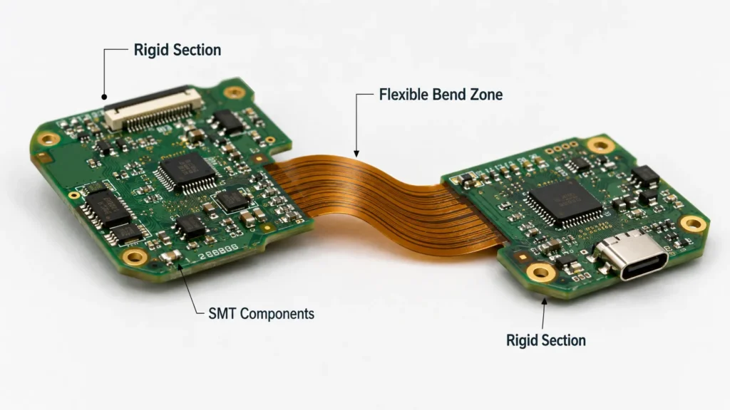
Rigid-flex reliability starts with the stack-up and bend-zone layout. Early DFM feedback can prevent material, routing, via, and transition problems before tooling.
Send Benlida your PCB files, stack-up, bend drawing, and BOM. Our engineering team can review the design and identify manufacturing risks.

