

Custom Flex PCB Fabrication
Custom Flexible PCB Manufacturer
Discuss your flexible PCB project with Benlida. Share the circuit files, stackup, connection details, and bend requirements so the construction and manufacturing scope can be reviewed for your application.
Static installation: Share the installed bend radius and the finished thickness of the bend zone.
Repeated movement: Define the motion, target cycles, speed, and operating environment.
Construction review: Review the layer structure, copper, coverlay, and stiffeners together. Bend suitability is project-specific.
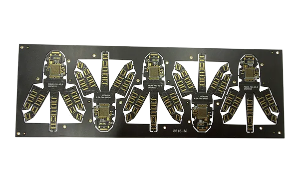
What Is a Flexible PCB?
A flexible printed circuit board, also called a flex PCB or FPC, uses a flexible insulating substrate to carry conductive circuits. It can fit into compact spaces or connect parts that move relative to each other. The construction must match the intended bending conditions.
Flex circuits may reduce wiring and connector use, depending on the assembly design. A thin or flexible circuit does not automatically provide long bend life or lower signal loss. These outcomes depend on the stackup, routing, assembly, and operating conditions.
Related services: PCB manufacturing services and rigid-flex PCB options. For a design comparison, read FPC vs. rigid PCB.
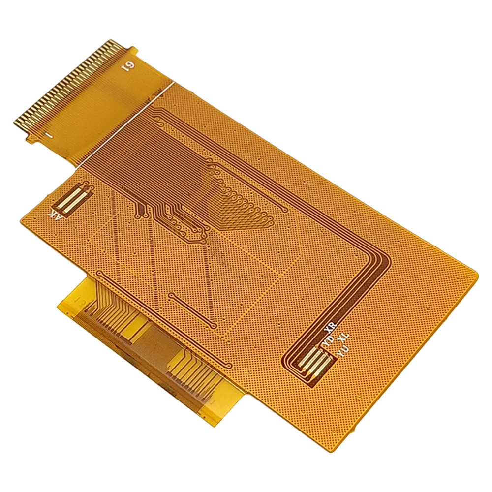
Our Flexible PCB Manufacturing Capabilities
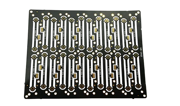
Benlida offers advanced flexible PCB manufacturing capabilities, including multi-layer designs, fine trace processing, flexible materials, and various surface finishing options. An experienced flexible PCB manufacturer like us offers a wide range of customized Flex PCB products that come with guaranteed quality control and flexible manufacturing options.
Layer Count
1-12 layers
Minimum Trace Spacing
3 mil (0.075 mm)
Flex Material
Polyimide, PET
Surface Finish
HASL, ENIG, OSP, Immersion Tin
Thermal Management
High thermal conductivity options
MOQ
1 pcs
Packaging
ESD Protection Materials, Moisture barrier bags, Bubble wrap, Corrugated cartons
Minimum Trace Width
3 mil (0.075 mm)
Minimum Via Diameter
75 μm (3 mils)
Copper Thickness
0.5-5 oz
Recommended Static Bend Radius
Single-layer ≥6×; double-layer ≥12×; multilayer ≥24× total thickness
Quality Standards
IPC-A-600, IPC-6013, ISO9001
OEM/ODM
available
Flexible PCB Manufacturing Process
The Benlida flexible PCB fabrication process incorporates all necessary steps, including design for manufacturing analysis, material selection, circuit creation, lamination, surface treatment, and testing. With proper manufacturing controls and modern manufacturing techniques, we can provide our customers with high-performance and high-quality customized flex PCBs.
1
FPC Design Review & Manufacturing Planning
Our engineers review the FPC design, bending requirements, circuit layout, and application conditions to define the optimal manufacturing approach for flexible circuit production.

2
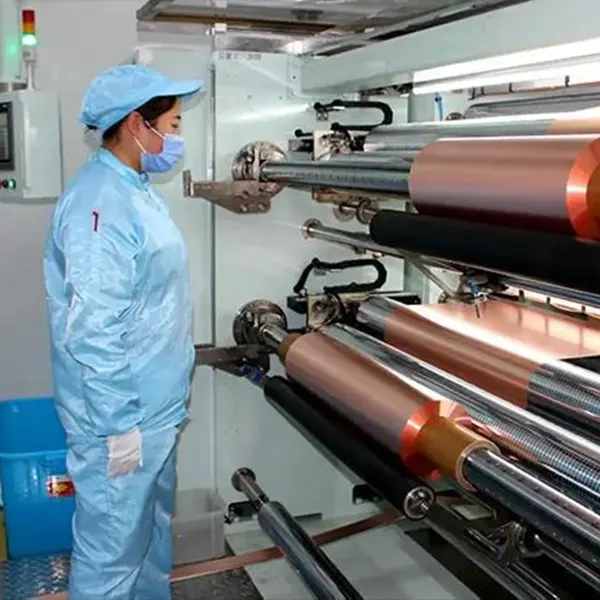
Flexible Material Selection & Preparation
High-quality flexible materials such as polyimide (PI) films and flexible copper clad laminates are selected based on thickness, flexibility, and electrical performance requirements.
3
Flexible Circuit Pattern Formation
Circuit patterns are transferred onto the copper layer through precision imaging and etching processes to create accurate conductive paths on the flexible substrate.
4
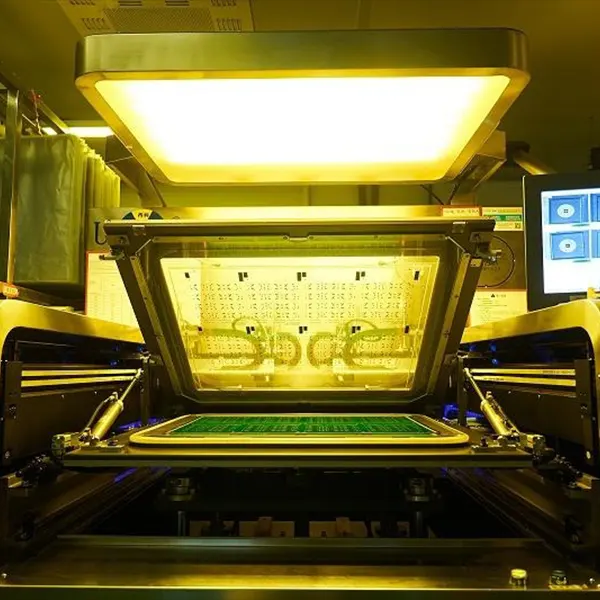
Micro Drilling & Via Formation
Precision drilling or laser processing is performed to create holes and vias, enabling reliable electrical connections for single-sided, double-sided, and multilayer FPC designs.
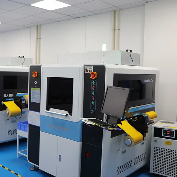
5
Flexible Layer Lamination
Copper layers, insulating films, and flexible materials are laminated together under controlled conditions to form a stable FPC structure while maintaining flexibility.
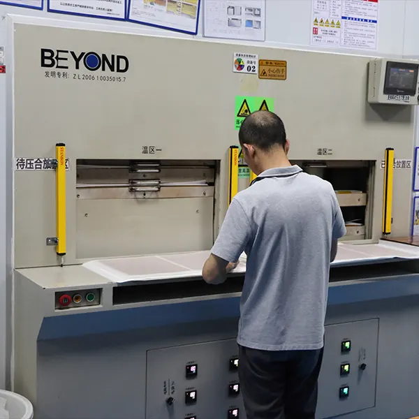
6
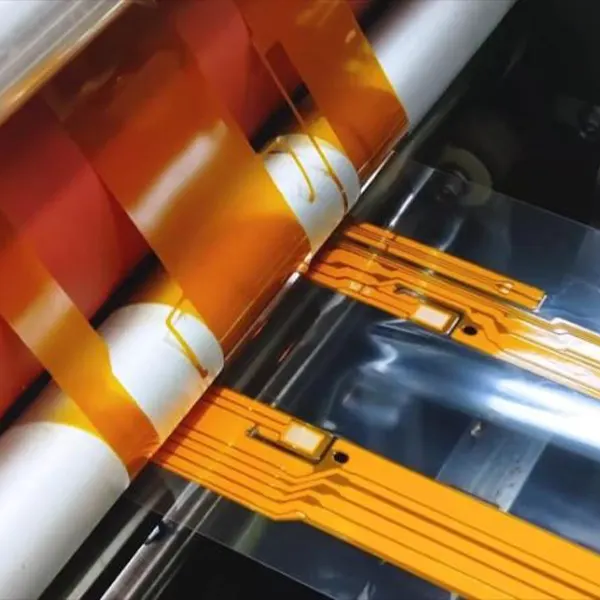
Coverlay Application & Circuit Protection
Coverlay films are applied to protect exposed circuits, improve insulation performance, and enhance durability during repeated bending or movement.
7
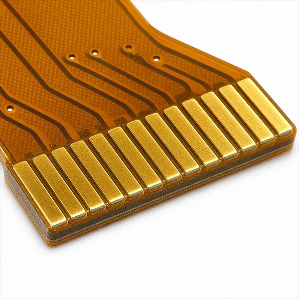
Surface Finishing & Connector Processing
Surface finishes such as ENIG or other suitable treatments are applied to improve solderability, while connector areas are processed according to assembly requirements.
8
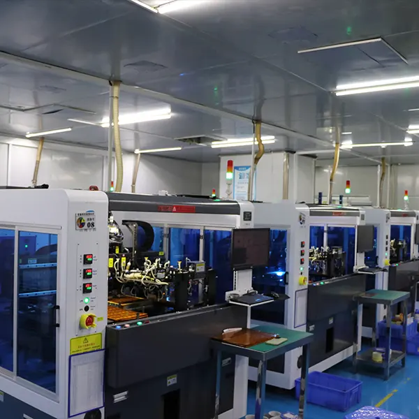
Reinforcement & Mechanical Enhancement
Stiffeners and reinforcement materials are added to specific areas when required, improving component support and connection reliability without affecting overall flexibility.
9
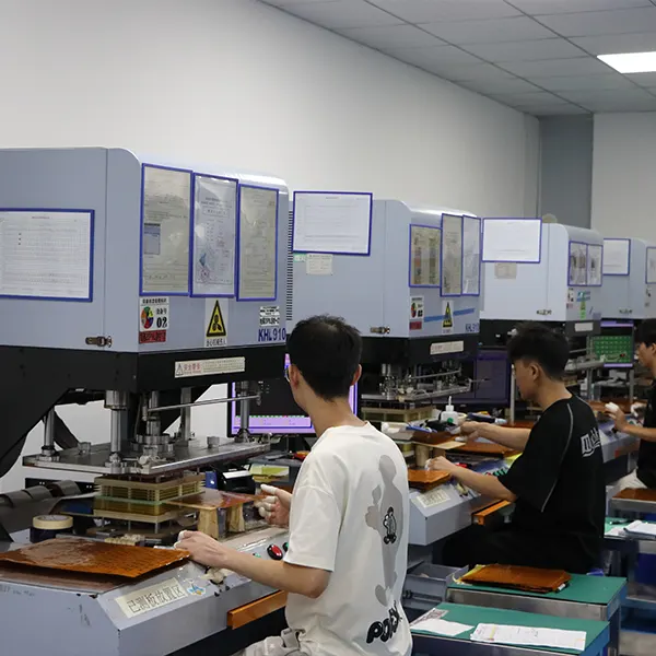
Electrical Testing & Flexibility Inspection
Each FPC undergoes electrical testing, dimensional inspection, and flexibility checks to ensure stable performance and reliable operation in flexible applications.
10
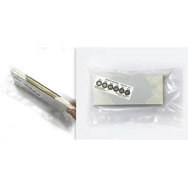
Packaging & Delivery Preparation
Finished FPC products are carefully packaged with protective materials, labeled according to customer requirements, and prepared for safe delivery.
Why Choose Benlida for Flexible PCB Solutions?
Professional FPC Manufacturing Expertise
As a company that has a lot of experience in manufacturing flexible circuits, Benlida is able to offer flexible PCB products for different sectors such as consumer electronics, automobiles, medical instruments, and many more. As an experienced fpc manufacturer, we have the capability to support multilayer designs, precision processing, and different flexible material requirements.
High-Precision Manufacturing & Quality Control
Our production process covers every critical stage, from design review and material selection to circuit fabrication, lamination, and final inspection. Owing to our highly developed flexible PCB manufacture capabilities, we practice stringent quality control for achieving steady electrical performance, durability, and product reliability.
Customized Flex PCB Solutions
Every application has unique requirements, and we provide tailored solutions based on customers’ designs, materials, layer structures, and performance needs. Our custom flex PCB services support projects from prototype development to mass production, helping customers achieve efficient and reliable flexible circuit solutions.
Reliable Production Capability
In the process of production, we ensure quality control, beginning from the preparation of materials, production, electrical testing, and final inspection. To our clients, we provide flexible OEM/ODM services and flexible production capacities, hence helping them in getting the best flexible PCB solutions from prototypes to large-scale production.
Flexible PCB Design Review Checklist
Review the circuit and mechanical requirements together. The following details help define the construction and identify questions before fabrication.
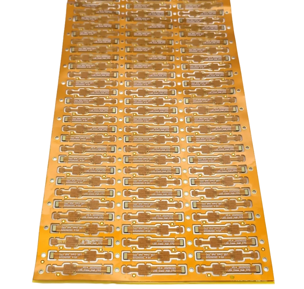
Define Static and Repeated Bending
Mark the bend zone and provide the inside bend radius and finished local thickness. For repeated movement, also specify travel, bend angle, cycles, speed, temperature, and how the flex is restrained. Do not use a single bend multiplier as a life guarantee.
Review Routing and Impedance
Consistent trace geometry supports impedance control. Impedance and signal loss also depend on the dielectric structure, copper, reference planes, frequency, and interconnections. Specify the target impedance and tolerance where required.
Coordinate Grounding and Shielding
Review return paths, reference conductors, and shielding with the signal requirements and bend conditions. Additional conductive layers can change both the electrical behavior and the mechanical construction.
Check Material and Assembly Compatibility
Specify the laminate grade, bonding system, coverlay, finish, and planned assembly process. PI and PET identify material families; they do not define interchangeable temperature or soldering limits.
Define Stiffeners and Connector Interfaces
Mark stiffener material, thickness, adhesive, and position. For a ZIF or other connector, provide the connector part number, contact orientation, and required finished tail thickness. Keep the bend-zone arrangement explicit in the drawing.
State Current and Thermal Conditions
Provide operating and peak current, duty cycle, permitted temperature rise, and cooling conditions. Review these together with copper thickness, trace geometry, and the complete flex construction.
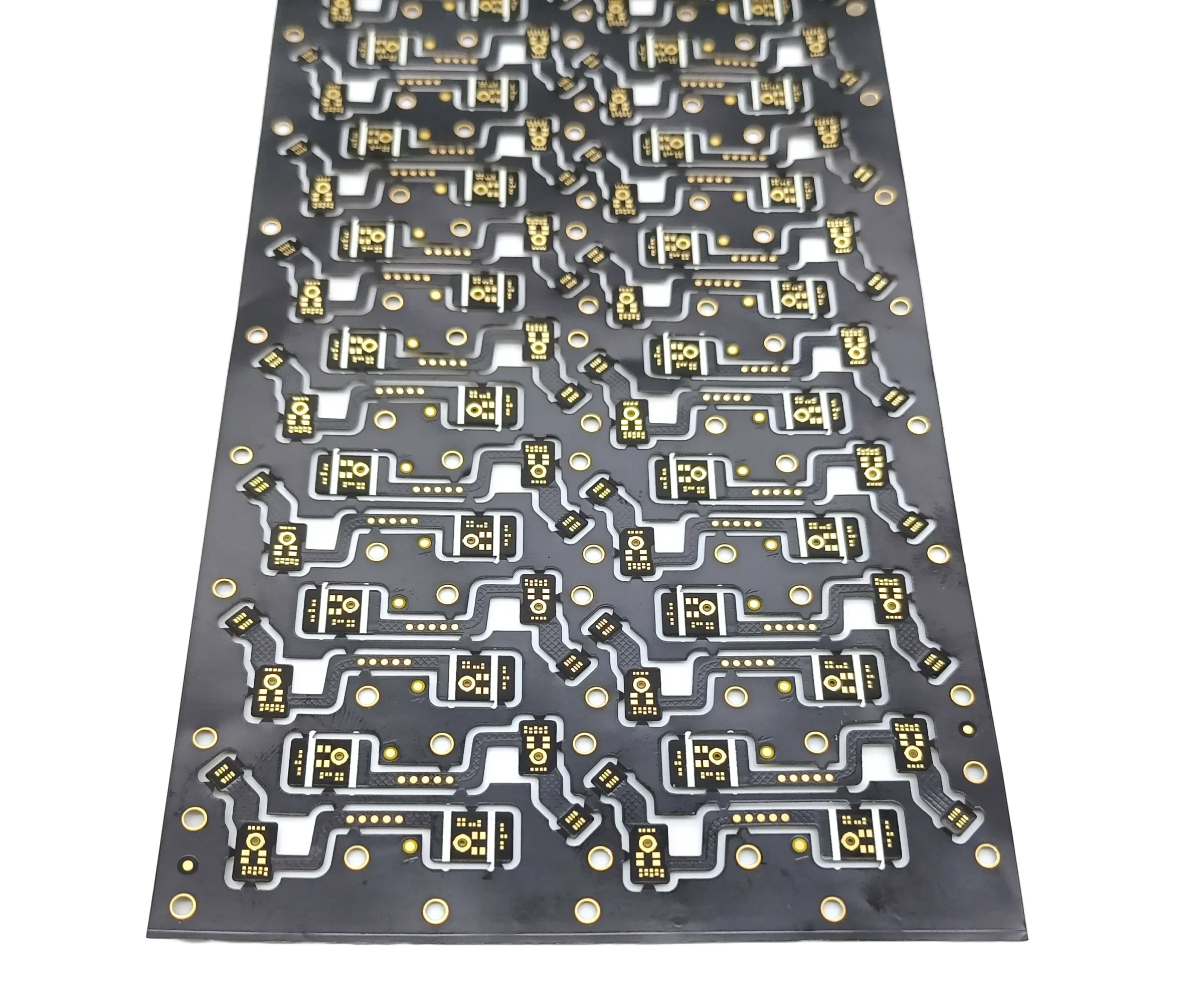
For an overview of the design choice, read FPC vs. rigid PCB.
Choose the Right Flex Circuit Structure
Start with the routing, connection, and bend requirements. Layer count describes the circuit construction; repeated bending describes a use condition and needs its own review.
Single-Sided Flex PCB
One conductive layer carries the circuit. Review the routing, contact access, and required local support for the intended installation.
Double-Sided Flex PCB
Two conductive layers provide routing on both sides. Where the layers need electrical connection, specify the plated interconnects and their position relative to the bend zone.
Multilayer Flex PCB
Three or more conductive layers support more complex routing. Review the stackup, finished thickness, bonding, and bend-zone construction together. More layers do not automatically improve bend life or signal performance.
Special Openings and Separated Layer Groups
Define special features with a fabrication drawing and cross-section. Show which layers are opened or removed, where bonding is required, and where layer groups remain separated. Names such as “hollow” or “layered” do not provide enough detail to establish the construction or manufacturing scope.
When to Consider Rigid-Flex
If the design needs integrated rigid sections and flexible interconnections, review rigid-flex PCB options. Rigid-flex is a separate construction choice and should not be treated as another flex layer-count category.
Flexible PCB Testing & Inspection
To ensure reliable performance, durability, and electrical stability, Benlida conducts comprehensive testing throughout the production process. These inspection procedures help verify the quality and reliability of custom flex PCB solutions for different application requirements.
Read about quality control and inspection and identify the checks needed for your flex PCB project.
Electrical Testing
Verify circuit continuity and electrical performance to identify potential open circuits, short circuits, or connection issues, ensuring reliable operation after flexible pcb manufacture.
AOI Inspection
Use automated optical inspection to detect defects in circuit patterns, traces, and surface conditions, helping maintain high precision during Flexible PCB production.
Dimensional Inspection
Check board dimensions, layer alignment, and critical design features to ensure each Flexible PCB meets customer specifications and design requirements.
Material & Surface Inspection
Inspect flexible substrates, copper layers, and surface finishes to confirm material reliability and support consistent performance across different applications.
Reliability Testing
Test the flexibility, resilience, and mechanical properties to make sure that the Flexible PCBs will be able to bend and withstand vibration and continuous use.
Final Quality Inspection
Conduct final inspection before shipment to verify product consistency and ensure each product meets the requirements expected from a reliable Flexible PCB manufacturer.
Applications of Flexible PCB
Flexible PCBs provide lightweight, flexible, and reliable circuit solutions that help different industries achieve compact designs, improved performance, and greater product reliability. Benlida supports custom flex PCB requirements for a wide range of applications with flexible design and manufacturing capabilities.
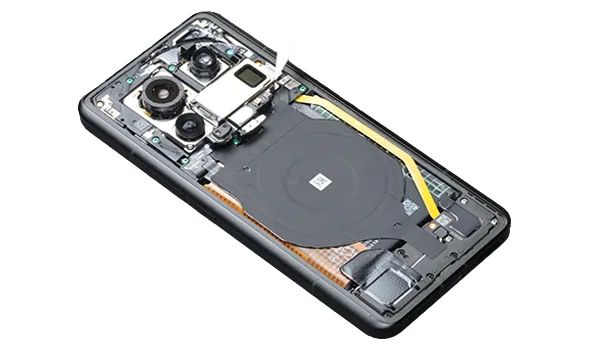
Consumer Electronics
Flexible PCBs allow the creation of thinner and lighter electronic products thanks to their ability to connect things within small spaces. They are widely applied in smartphones, wearables, tablets, and other mobile electronics.
Automotive Electronics
In the automobile industry, the use of Flexible PCBs can assist in reducing wiring complications and improving connection reliability. The flexibility and strength of the board allow it to be applied in the manufacture of displays, sensors, control units, and intelligent cars.
Medical Devices
Flexible PCBs support the development of smaller and more reliable medical equipment by enabling compact circuit designs and stable electrical performance. They are commonly used in wearable medical devices, monitoring equipment, and diagnostic systems.
Industrial Equipment
Flexible PCBs provide reliable circuit solutions for industrial applications that require durability, vibration resistance, and efficient space utilization. They help improve system integration and performance in automation equipment and control systems.
Aerospace & Defense Electronics
The flexible board is appropriate for applications that require lightness, durability, and complicated circuits. The flexibility and strength of the board make it fit for aerospace applications.
Flexible PCB FAQ
Share your design, quantity, and application with Benlida for a project review. The construction, manufacturing scope, engineering support, and schedule should be confirmed in the quotation.
PI and PET are material families, not complete construction specifications. Provide the material grade, dielectric thickness, bonding system, finish, and assembly conditions so compatibility can be reviewed.
A flex PCB uses a flexible substrate. A rigid PCB uses a rigid base. A rigid-flex PCB integrates rigid and flexible sections. Select the construction based on the mechanical arrangement, routing, and connection requirements.
The suitable layer count depends on the routing, stackup, copper, thickness, and bend requirements. Review these features together. A layer-count claim alone does not establish whether a specific construction is manufacturable.
Provide the inside bend radius, finished thickness at the bend zone, and installed geometry. Also state whether the circuit is bent during assembly or moves repeatedly. Confirm the radius for the complete construction instead of relying on a universal multiplier.
It may be suitable if its construction matches the motion. Provide the bend geometry, target cycles, speed, restraint, and environment. Agree on a test plan and failure criterion before treating bend life as validated.
Provide the stiffener material, thickness, adhesive, location, and tolerances. For a ZIF connection, include the connector part number, contact orientation, and required finished tail thickness.
Define circuit connectivity, critical dimensions, and any required material or surface checks. Confirm inspection coverage and records. Repeated-bend or environmental validation needs a project-specific plan and is separate from routine inspection.
Provide Gerber or ODB++ data, drill data, a fabrication drawing, and the current revision where available. Include quantity, stackup, finished thickness, copper, finish, bend requirements, coverlay, stiffeners, and connection details.
Yes. Describe the application, available space, connection method, intended motion, approximate quantity, and any open questions. Incomplete files can support an initial discussion; a production release requires confirmed manufacturing information.
Construction, quantity, materials, tooling, inspection, and any assembly work affect the quotation. Provide the requested delivery date and project stage. Confirm minimum order quantity, engineering charges, and the schedule with the agreed scope.
Identify assembly as a separate scope. In addition to the bare-board files, provide the BOM, pick-and-place data, assembly drawing, and any test or programming requirements. Review these through the PCB assembly services route.
Key Features and Advantages of Flexible PCB
Flexible PCB provides good flexibility, light weight, and high reliability, which makes it the best fit for present-day electronics with complicated designs. With advanced flexible PCB manufacturing capabilities, Benlida provides reliable FPC solutions that support various application requirements.
Lightweight and Flexible Design
Flexible PCB uses flexible substrates that allow bending, folding, and three-dimensional installation, making it suitable for compact devices and space-limited applications.
Space Saving and Weight Reduction
Compared with traditional rigid PCBs, Flexible PCB features a thinner and lighter structure, helping reduce connectors and wiring while enabling more efficient product designs.
High Reliability and Bending Performance
Flexible PCB provides excellent mechanical flexibility and durability, allowing stable operation in applications exposed to bending, vibration, or repeated movement.
Excellent Signal Performance
With precise circuit design and stable material properties, Flexible PCB supports reliable signal transmission while helping reduce interference and signal loss.
Flexible Design Adaptability
Flexible PCB can adapt to irregular spaces and complex assembly requirements, providing custom flex PCB solutions for diverse electronic product designs.
Core Structural Types of Flexible PCB
Flexible PCBs can be organized under various structures depending on the number of layers, circuit complexity, and the needs of the application. Knowing how flexible PCBs are structured makes it easy to find the right solution that suits your product. Benlida provides custom flex PCB solutions with various structural options to meet different design and performance requirements.
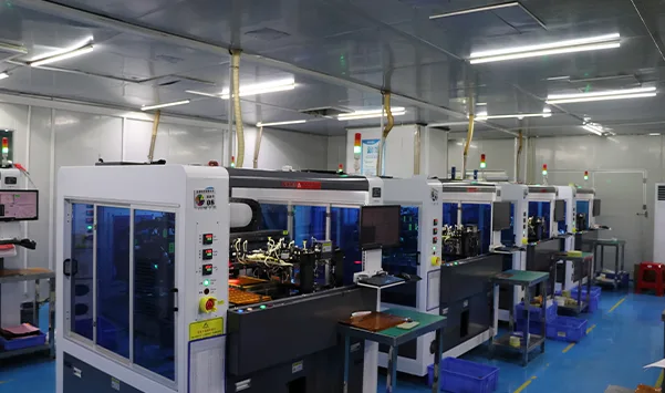
Single-Sided Flexible PCB
A single-sided Flexible PCB is a flexible printed circuit board with only one layer of conductive copper on its substrate. It has a simple structure and design, offers weight savings, and is economical.
Double-Sided Flexible PCB
A double-sided Flexible PCB is a type of flexible PCB with conductive materials on both sides of its substrate, joined by plated vias. The double-sided flex PCB is more advanced compared to the single-sided PCB.
Multi-Layer Flexible PCB
A multi-layered Flexible PCB is made up of three or more layers of conductors combined to form circuits that will be denser and have high functionality. It is often used where there is a need for complex wiring and increased electrical performance.
Hollow Flexible PCB (Windowed Flex PCB)
A hollow Flexible PCB has particular openings in the flexible circuit for improved assembly, weight reduction, and specific mechanical/assembly requirements.
Layered Flexible PCB
A layered flexible PCB uses a multi-section or separated layer structure to optimize circuit arrangement and mechanical performance. This design helps achieve better space utilization and is suitable for applications requiring specific thickness, flexibility, or structural configurations.
Request a Quote for Your Flex PCB Project
Share the information you have. Identify any open requirements so the next review can focus on the construction, bend conditions, and manufacturing scope.
If Your Design Files Are Ready
Include Gerber or ODB++ data, drill data, the fabrication drawing, and the current revision. State the quantity, layer stackup, finished thickness, copper requirements, surface finish, impedance requirements if any, and requested delivery date.
Add the Flex-Specific Details
Mark bend zones, inside bend radius, coverlay openings, stiffener details, and connector requirements. For repeated movement, provide the travel, bend angle, target cycles, speed, restraint, and operating environment.
If Your Files Are Not Ready
Describe the application, available space, connection method, intended movement, approximate quantity, and the questions you need to resolve. You can start with a project description.
If Assembly Is Also Required
Add the BOM, pick-and-place data, assembly drawing, and test or programming requirements. Review PCB assembly services as a separate scope from bare-board fabrication.
Order quantity, engineering or tooling charges, and schedule are confirmed in the quotation. Before sharing confidential files, contact us to agree on the transfer method.