

PCB Panelization Guide — V-Score, Tab Routing & Break-Away Methods
What Is PCB Panelization?
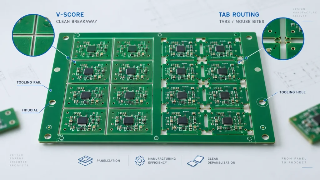
PCB panelization groups individual boards into a larger layout for production and handling. For SMT assembly, V-score grooves and tab routing are common ways to keep boards connected until separation. Choose the method around board shape, component clearance, line requirements, and acceptable mechanical stress.
A fabrication panel is the working panel used to manufacture bare PCBs. An assembly array is the layout delivered for component assembly. Several assembly arrays may fit within one fabrication panel. This guide focuses on rigid-board assembly arrays.
Panelization helps small boards move through the PCB assembly process as a stable group. After assembly, depanelization separates the populated boards, or PCBAs. A useful panel must work during solder paste printing, placement, soldering, inspection, and final separation—not just fit more units into a rectangle.
V-Score Panelization — Process and Limitations
V-scoring, also called V-cut, creates grooves along planned separation lines. Usually, grooves enter from both board faces. A thin section of material remains between them to hold the boards together.
Conventional rotary scoring generally follows straight lines across a panel. This suits rectangular boards arranged in rows and columns. Some suppliers offer interrupted, or jump, scoring. Multi Circuit Boards’ V-scoring guidance explains why these interrupted cuts still need blade entry and exit space.
Do not set score depth as a fixed percentage for every board. Too little remaining material can weaken the array during handling. Too much can increase the force needed to separate it. Agree the remaining thickness and tolerance with the fabricator and depaneling team.
A V-score PCB layout also needs clearance from copper, components, and overhanging connectors. Check the groove geometry and the separation tool on both sides of the board. Closely packed board outlines do not mean parts can sit directly beside the cutting path.
Tab Routing and Break-Away Perforation
Tab routing mills channels around each board while leaving small connecting bridges, called tabs. These bridges join neighboring boards or connect a board to an outer rail. Routing can follow curves, cutouts, and irregular outlines that do not suit a simple scored grid.
Tabs may be solid or perforated, as described in MADPCB’s route-and-retain explanation. Perforated tabs contain small holes called mouse bites. These holes weaken the bridge for controlled separation; they are not electrical vias. Solid tabs can instead be cut with suitable depaneling equipment.
Place tabs where they support the board without obstructing connectors or critical enclosure interfaces. A removed tab may leave a small projection or rough edge. Define the allowed edge condition and any trimming requirement on the drawing.
More tabs can increase support but also add separation work. Fewer tabs can leave a narrow or heavy assembly poorly supported. Review their number and position together with the cutting sequence. A breakaway PCB panel is not automatically safe to snap apart by hand.
Panel Size and Spacing Design Rules
There is no single panel size or spacing rule for every production line. LPKF’s panelization guidelines relate panel dimensions to equipment limits and board spacing to the separation tool. Treat a supplier’s published dimensions as that supplier’s process rules, not universal limits.
Confirm the Complete Assembly Envelope
The fabricator’s largest production panel is not necessarily the assembler’s largest usable array. Confirm minimum and maximum dimensions across printing, placement, reflow, inspection, testing, and depaneling. Include the outer rails when stating overall panel dimensions.
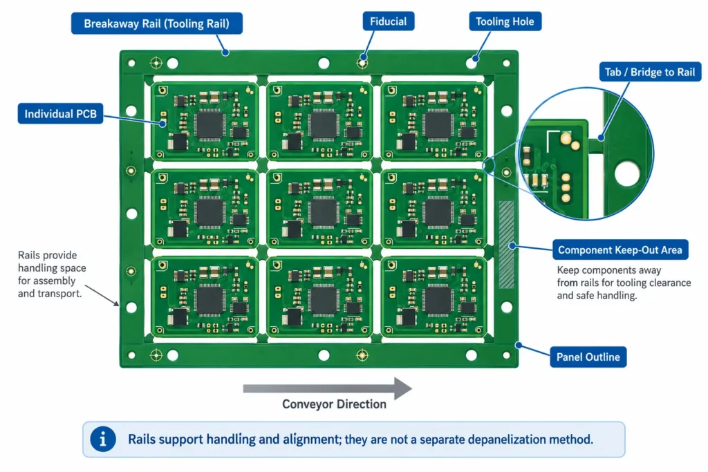
Breakaway rails, or tooling rails, provide handling space and can carry alignment marks, called fiducials, plus tooling holes. They are support features, not a separate depanelization method. Eurocircuits’ panel guidance distinguishes these borders from the methods used to separate individual boards.
Agree which edges need rails and how much clamping space the line requires. Include underside components and connector overhangs. A panel that fits the conveyor can still collide with a clamp or lack support during printing.
Approve Spacing and Manufacturing Data
For tab-routed panels, allow a channel that suits the router diameter, tool access, and final edge tolerance. Adjacent V-scored boards may share a nominal outline with no routed gap. That does not remove copper, component, or blade-clearance requirements.
Record these PCB panel design rules before release:
- Overall panel dimensions, unit count, orientation, and delivery quantity in panels or individual boards.
- Board outlines, routing channels, score lines, tab locations, and finished-edge requirements.
- Rail widths, conveyor direction, tooling holes, fiducials, and clear areas around them.
- Material, board thickness, copper keepouts, component heights, and overhanging parts.
- Panel drawing revision, coordinate origin, inspection access, and approved separation method.
During Gerber file preparation, identify whether the data describes one board or the complete array. If the supplier will create the panel, approve its drawing before production. Keep assembly coordinates and stencil data aligned with the approved revision.
Choosing Panelization Method by Board Shape
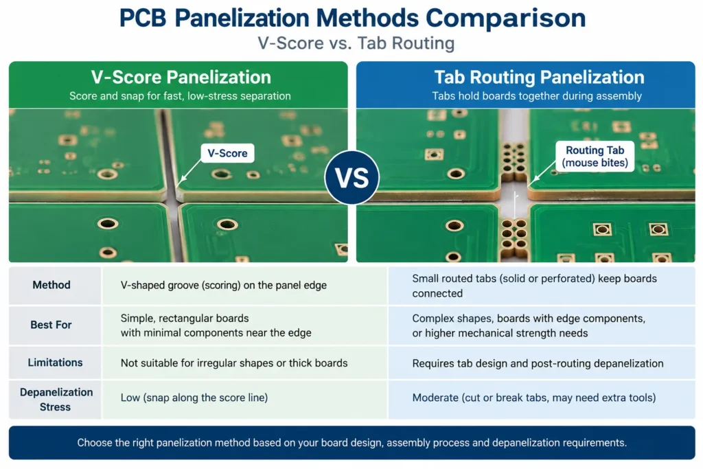
Start with the outline, then check the populated assembly. V-score often suits repeated rectangular boards. Tab routing offers more freedom for curved edges, slots, or uneven shapes. A mixed design can use scoring for straight sections and routing elsewhere, subject to supplier approval.
The comparison below separates panel construction from the force applied during final separation. Neither method has one fixed stress level.
| Method | Best For | Limitations | Depanelization Stress |
|---|---|---|---|
| V-score | Regular arrays with straight separation lines. | Requires suitable score geometry and blade clearance; awkward for complex outlines. | Depends on remaining thickness, support, and separation equipment. |
| Tab routing with perforated tabs | Irregular outlines held by breakaway bridges. | Needs routing space and planned tab positions; edge remnants may need attention. | Bending during breakout can stress nearby parts; use a validated method. |
| Tab routing with solid tabs | Irregular outlines intended for tool-cut separation. | Needs cutter access, suitable fixtures, and an approved cutting sequence. | Supported routing can limit bending, but is not stress-free. |
For example, a rectangular board with an overhanging connector may need routing clearance despite its simple shape. Likewise, a densely populated board may need a different fixture or separation method. Evaluate component access before choosing the tightest possible array.
Depanelization and Its Effect on Component Stress
Depanelization can bend the board and strain components, copper traces, or solder joints. Multilayer ceramic capacitors, or MLCCs, deserve particular attention. Murata’s MLCC layout guidance shows how board bending, component orientation, and proximity to separation points affect cracking risk.
Keep brittle parts away from separation points where practical. Review their orientation against the expected bending direction. If space is limited, discuss layout changes or a lower-stress separation process before release.
ASYS’s depaneling guidance explains why excessive mechanical stress can damage populated boards. Supported routing can reduce bending, but tool condition, fixture design, and handling still matter. Avoid twisting an assembled board to release its tabs.
For sensitive assemblies, agree how the process will be validated, including any board-strain measurement and acceptance limits. Inspect the finished edges and verify required product checks after separation. Passing electrical tests while boards remain in the panel does not prove that later depanelization caused no damage.
FAQ
What is the difference between V-score and tab routing?
V-score uses grooves along separation lines and leaves a thin material web. Tab routing cuts around the board while retaining connecting tabs. V-score commonly suits straight-edged arrays. Tab routing accommodates more complex shapes. The final choice also depends on component clearance and the available depaneling equipment.
What is the minimum board spacing for panelization?
There is no universal minimum. Tab routing needs space for the routing tool and required tolerances. Some V-score layouts have no routed gap between adjacent outlines, but still need copper and component clearance. Obtain approved spacing from the fabricator, assembler, and depaneling team.
Does panelization method affect component placement near edges?
Yes. Components must clear grooves, tabs, cutting tools, and fixtures. Fragile parts may also need separation from areas that bend during depanelization. Check both board faces and any connector overhangs. A copper-to-edge rule alone is not a component-placement rule.
Who decides the panelization method — the designer or the manufacturer?
It should be agreed jointly. The designer provides outline and component constraints. The fabricator confirms board-processing limits, while the assembler confirms line and separation requirements. The supplier may propose the layout, but the responsible customer team should approve the controlled drawing before production.
Planning Panelization for SMT Production?
Send Benlida your fabrication files, board outline, assembly drawing, component heights, and proposed panel layout. Include the revision, build quantity, and any sensitive parts or critical edges. When discussing PCB manufacturing services, ask engineering to review panel feasibility and confirm the supported separation method. Agree project-specific dimensions and responsibilities before release.