

Professional Heavy Copper PCB Manufacturer
Heavy Copper PCB & Custom Copper Clad PCB Board Solutions
We specialize in manufacturing heavy copper PCBs with up to 6 oz copper thickness, delivering high-current and reliable PCB solutions for power electronics, automotive, and industrial applications.
Typically handles 10-30A depending on trace width
Can safely carry 50-100A per layer
6 oz copper
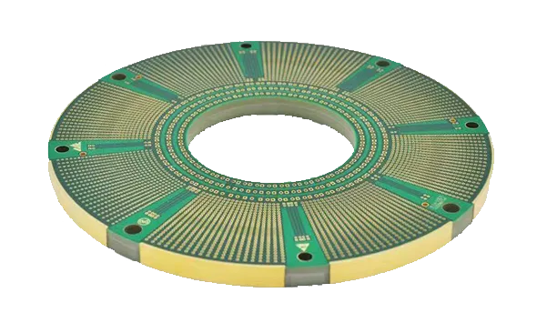
What is Heavy Copper PCBs?
Heavy Copper PCB is a type of printed circuit board that uses copper with a thickness of at least 3 oz/ft² (105 μm) in its outer and/or inner layers.
The heavy copper PCBs are manufactured specially for those applications where a high current capability, excellent thermal characteristics, and strong mechanical strength are required. As compared to a regular 1 oz copper PCB, a heavy copper PCB gives better results in terms of lower electrical resistance, better heat distribution, and reliability under harsh conditions.
We are leading heavy copper PCB manufacturer offering custom solutions with our high-quality copper-clad PCB board.
Related services and board types: Explore our PCB Manufacturing Services.
Our Heavy Copper Manufacturing Capabilities
Benlida offers reliable solutions for heavy copper PCB manufacturing services with advanced production facilities, providing services on copper thicknesses ranging from 3oz to 6oz as standard and 20oz for custom designs. As a trusted heavy copper PCB supplier, we offer multilayer construction, precision drilling, various surface finishes, and OEM/ODM services to meet the requirements of high-power and high-reliability applications.
Copper Thickness
3oz- 6oz standard; custom heavy copper options available (up to 20oz on request)
Minimum Trace Width/Spacing
≥150μm (6 mil) typical for heavy copper
Aspect Ratio
Up to 8:1 depending on structure
Layer Alignment Tolerance
±75μm typical
Solder Mask
High-temperature resistant solder mask
Via Technology
Through-hole, filled vias, heavy copper vias
OEM/ODM
available
Board Thickness
0.8mm-6.0mm standard; thicker constructions available
Minimum Drill Size
≥0.3mm (12 mil); precision drilling
Multilayer Capability
Up to 12 layers or more
Surface Finish Options
HASL, Lead-Free HASL, ENIG, OSP, Immersion Silver, Immersion Tin
Surface Roughness Contro
Optimized for adhesion and performance
MOQ
1pc
Packaging
ESD Protection Materials, Moisture barrier bags, Bubble wrap, Corrugated cartons
Heavy Copper PCB Manufacturing Process
Our company manufactures heavy copper PCBs using a detailed process that entails materials preparation, inner/outer layer imaging, lamination, drilling, copper plating, surface finishing, and inspection. This ensures that our heavy copper printed circuit boards have well-defined circuitry.
Heavy copper printed circuit board products from Benlida are manufactured using superior technology and quality control. Therefore, our customers benefit from printed circuit boards with good electrical and thermal conductivity.
1
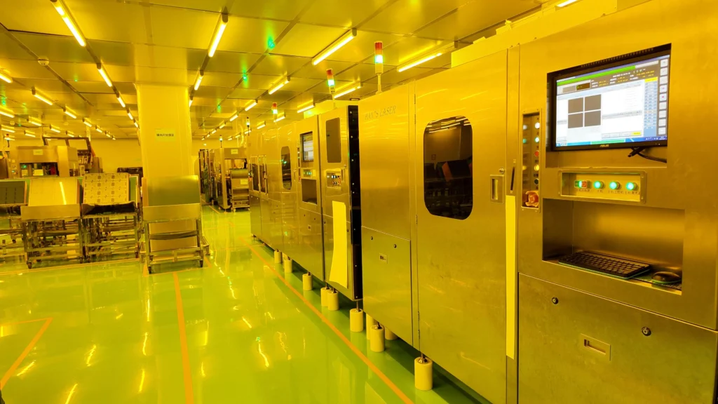
Material Preparation
Select high-performance base materials, including high-Tg laminates and 3 oz or thicker copper foil, to ensure excellent electrical performance, thermal management, and long-term reliability.
2
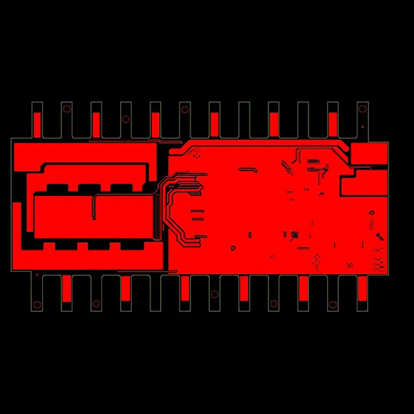
Inner Layer Imaging & Etching
Circuit patterns are precisely transferred onto the copper layers using photolithography, followed by controlled etching to produce accurate trace geometries in thick copper.
3
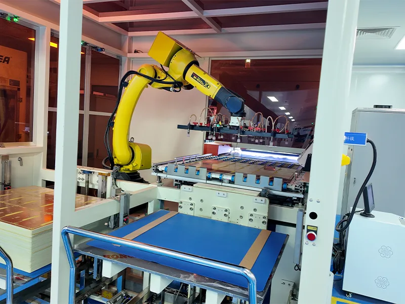
Layer Lamination
Multiple PCB layers are precisely stacked and laminated under controlled heat and pressure to create strong bonds and ensure a void-free, highly reliable multilayer structure.
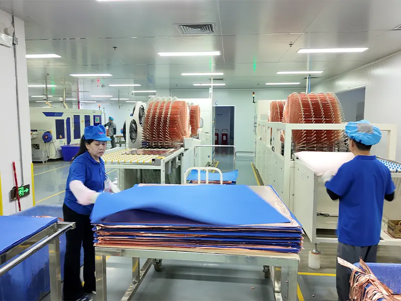
4
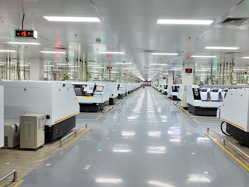
Drilling & Via Formation
High-precision mechanical or laser drilling creates accurate vias and holes, ensuring reliable interlayer connections and precise alignment in thick copper multilayer PCBs.
5
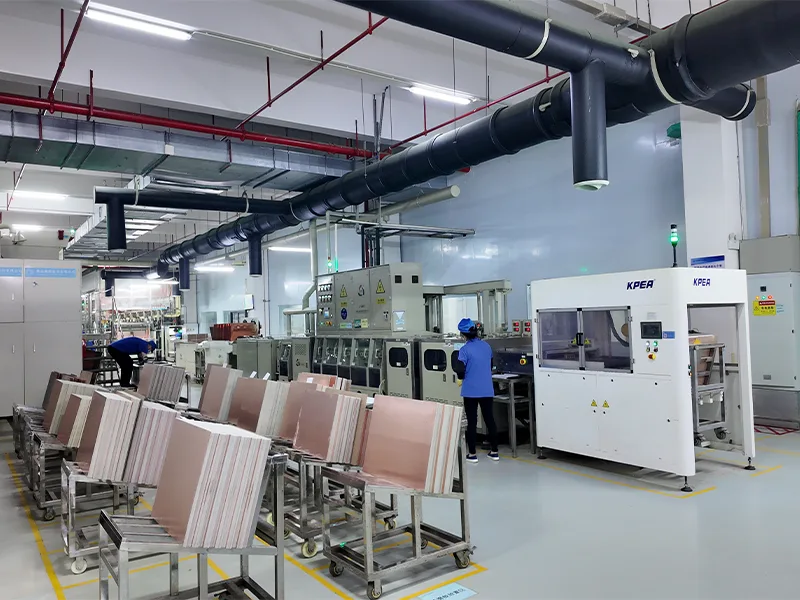
Copper Plating
Electroplating deposits additional copper onto vias and traces, enhancing conductivity, increasing copper thickness, and ensuring reliable interlayer connections.
6
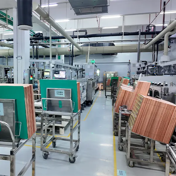
Outer Layer Patterning
The final circuit pattern is formed through precision imaging and controlled etching, ensuring accurate trace geometry and consistent quality in heavy copper PCBs.
7
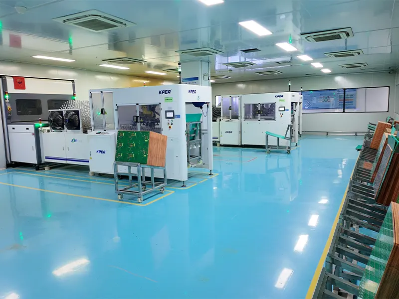
Surface Finish
Apply surface finishes such as HASL, ENIG, or Immersion Silver to protect exposed copper, improve corrosion resistance, and ensure excellent solderability.
8
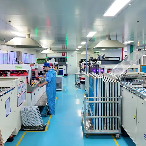
Solder Mask & Silkscreen
Apply a high-temperature solder mask to protect the PCB surface and add silkscreen markings for clear component identification and assembly guidance.
9
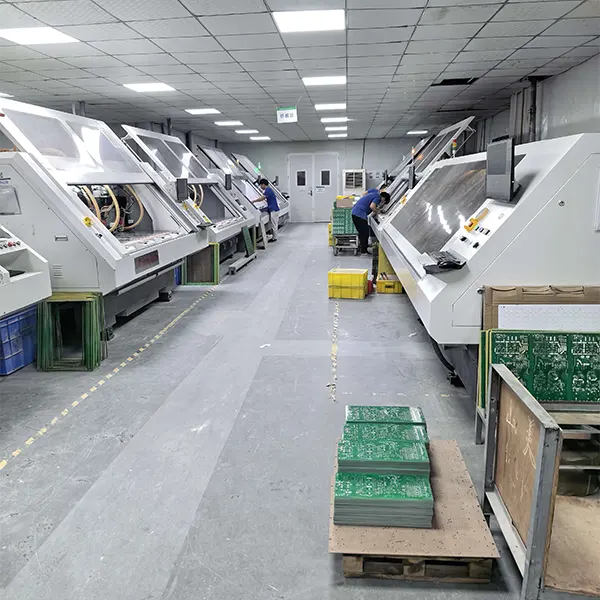
Routing & Profiling
The PCB is separated into its final dimensions using precision CNC routing or V-scoring, ensuring accurate outlines and clean, smooth edges.
10
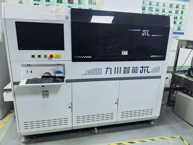
Testing & Inspection
Perform comprehensive inspections, including electrical testing, AOI, and X-ray inspection, to verify circuit integrity, detect defects, and ensure reliable internal structures.
Why Choose Us?
Professional Manufacturing
Through our wide experience in the manufacture of heavy copper printed circuit boards, Benlida is able to offer quality solutions thanks to modern manufacturing technologies and high-quality standards.
Flexible Customization Capability
We support standard copper thickness from 3oz to 6oz and custom heavy copper designs up to 20oz, along with multilayer structures, various surface finishes, and OEM/ODM services to meet different project requirements.
Strict Quality Control System
We make sure that we complete quality checks through AOI, X-ray inspection, and electrical testing throughout the process, from materials to final products.
Reliable Manufacturing Partner
As one of the trusted heavy copper PCB manufacturers, we support prototype and mass production with efficient delivery and customized solutions to help customers achieve their PCB development goals.
Heavy Copper PCB Advantages
Copper clad PCB boards with heavy copper layers feature great electrical, thermal, and mechanical properties suitable for challenging electronic applications. Unlike regular PCBs, the Heavy Copper PCBs have better current-carrying capacity, heat dissipation capabilities, and reliability due to their design features.
High Current Carrying Capacity
The Heavy Copper PCBs consist of copper thickness and enable them to conduct higher currents without generating too much heat. Hence, the Heavy Copper PCBs are useful for devices requiring a stable power supply.
Superior Heat Dissipation
The robust copper structure of a copper clad PCB board enhances heat dissipation by spreading heat more efficiently across the PCB. This reduces hotspots, improves system stability, and helps minimize the need for additional cooling solutions.
Enhanced Mechanical Strength
With heavy copper traces and planes on a PCB, there is improved mechanical robustness of the printed circuit board because of increased resistance to vibrations, heat, and tough environments. Heavy copper printed circuit boards are used in various industries like automobile, aerospace, and more.
Improved Reliability and Longevity
Because of the reduced electrical resistance and thermal stress, heavy copper PCBs offer reliability and longevity. Their performance remains stable at high current, high temperature, and under difficult operating conditions.
Simplified Circuit Design
The high current-carrying capacity of each trace eliminates the need for parallel routing or an extra layer of the PCB.
Better Resistance to Thermal Cycling
Heavy Copper PCBs are known to withstand thermal cycling well, thereby providing consistent functionality in applications that have many power cycles and difficult operating conditions.
Higher Power Density
Because of the heavy copper construction, high currents can be delivered in small spaces, making it possible to design high-power-density boards without sacrificing functionality, reliability, and thermal dissipation capacity.
Reduced Risk of Failure
The strong build with copper assures no issues like degradation of trace, delamination, and failure of via; hence, assuring efficient functioning of the PCB in critical applications.
Flexibility for Harsh Environments
Heavy Copper PCBs are capable of functioning successfully in conditions of extreme temperature, humidity, vibration, and even chemical exposure.
Heavy Copper PCB Design Guides
Heavy copper printed circuit boards (PCBs) are created specifically for high current applications and need to take into account many factors, including copper weight, trace configuration, thermal management, layering, and manufacturing considerations. Designing techniques can help in designing an effective electrical and thermal design that will last for many years.
Designers can be assured of optimized structures and reliable performance through adherence to proven design guidelines and collaboration with experienced heavy copper PCB manufacturers.
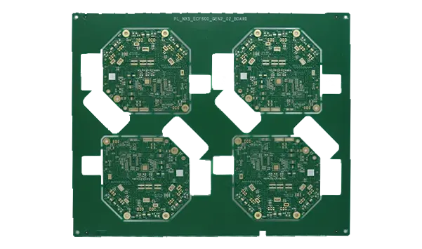
Heavy copper PCBs are designed for high-current and high-power applications, requiring careful consideration of copper thickness, trace geometry, thermal management, layer stackup, and manufacturability.
Optimize Trace Width for Current Capacity
It will not be enough to rely solely on the use of thicker copper. Traces must be designed based on the amount of current being used and the allowable temperature rise.
Avoid Over-Specifying Copper Thickness
Too much copper thickness can complicate manufacturing processes and make them costly. Heavy copper should be applied when an increase in the current-carrying capacity is required; otherwise, regular copper should be used.
Maintain Proper Trace Spacing
It should be noted that proper spacing between conductors needs to be taken into consideration in order to avoid electrical breakdown and ensure proper insulation, particularly for high voltage applications.
Use Smooth Corners and Gradual Transitions
Avoid sharp edges on heavy copper traces to avoid current crowding. Rounded corners and smooth width changes must be used.
Allow for Thermal Expansion
Heavy copper layers experience different expansion rates during temperature changes. Proper clearances and suitable material selection help reduce thermal stress and prevent delamination in multilayer copper clad PCB board structures.
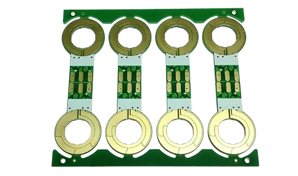
Proper design practices help ensure reliable electrical performance, efficient heat dissipation, and long-term durability.
Optimize Via Design for High Current
Use larger vias or multiple vias in parallel to support high-current transmission. Ensure adequate copper plating thickness to improve reliability and prevent via failure caused by thermal stress.
Plan Layer Stackup Carefully
Properly separate power, ground, and signal layers within the stackup to optimize electrical performance, minimize noise interference, and improve thermal management.
Consider Manufacturability
Heavy copper PCBs require specialized manufacturing processes and tighter fabrication control. Working closely with experienced manufacturers ensures that trace widths, spacing, and via structures are optimized for reliable and cost-effective production.
Control Surface Roughness and Plating
Surface roughness and copper plating uniformity play a critical role in electrical performance and long-term PCB reliability. Define appropriate specifications based on application requirements and performance goals for copper clad PCB board structures.
Product Testing & Quality Control
To ensure the stability and reliability of Heavy Copper PCB products in high-current and high-power applications, Benlida implements a comprehensive quality control system covering material inspection, production monitoring, and final testing. As experienced heavy copper PCB manufacturers, we apply strict inspection procedures to maintain consistent quality and reliable performance.
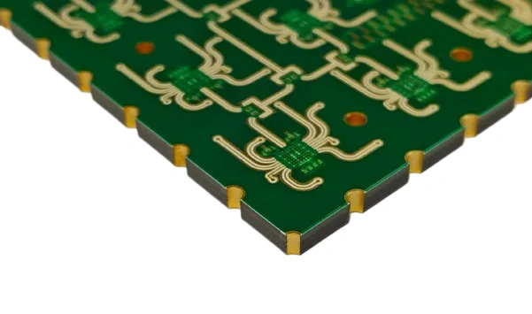
Electrical Performance Testing
Electrical testing is conducted to check the performance of the circuits for proper connection and insulation.
AOI (Automated Optical Inspection)
The AOI testing procedure involves automatic scanning of the PCB circuits to detect any possible open circuits, shorts, and problems with patterns.
X-Ray Inspection
X-Ray inspection is performed to examine internal structures, including multilayer connections, for quality, and hidden defects, ensuring reliable internal performance.
Copper Thickness and Structure Inspection
Copper thickness, trace structures, and critical dimensions are carefully controlled to ensure Heavy Copper PCB products meet required specifications and performance standards.
Final Quality Inspection
Prior to shipment, all the PCB is subjected to a thorough inspection process, which includes visual inspection, dimension verification, and performance testing to guarantee reliable quality.
Heavy Copper PCB Applications
Heavy Copper PCBs are widely used in industries that require high current carrying capacity, excellent thermal management, and long-term reliability. As experienced heavy copper PCB manufacturers, Benlida provides reliable Heavy Copper PCB solutions based on high-quality copper clad PCB board materials to meet the needs of high-power applications and demanding operating environments.
Power Electronics
Heavy Copper PCBs are commonly used in power modules, inverters, and power conversion equipment. Their enhanced current capacity and heat dissipation capabilities help ensure stable and efficient system operation.
Automotive Electronics
For electric cars, motor controllers, and battery management systems, Heavy Copper PCBs prove to be very reliable and offer good thermal properties, which are required in the automotive environment.
Industrial Equipment
Heavy Copper PCBs support industrial automation equipment, motor drives, and control systems where high current handling and long-term operational stability are essential.
Renewable Energy Systems
Heavy Copper PCBs are suitable for solar inverters, energy storage systems, and power management equipment, providing reliable circuit performance for high-power energy applications.
Aerospace & High-Reliability Applications
With enhanced mechanical strength and resistance to harsh conditions, Heavy Copper PCBs meet the reliability requirements of aerospace and other mission-critical applications.
FAQ
3oz-6oz copper thickness is the common one in heavy copper PCBs; however, they may use up to 20oz copper if requested by customers.
The Heavy Copper PCB is a kind of printed circuit board that uses a copper thickness of 3 oz/ft² or greater on its external or internal layers. It is better than ordinary PCBs because it has an increased capacity for current flow, heat dissipation, and mechanical durability. As experienced heavy copper PCB manufacturers, Benlida provides reliable solutions for demanding electronic projects.
The Heavy Copper PCBs can be applied to fields like power electronics, automotive electronics, industrial control, renewable energy, and aerospace due to their superior electrical current-carrying capability and reliable performance.
The use of Heavy Copper PCBs will make it easier to have higher current capacity, superior thermal performance, mechanical strength, and longer service life.What is more, Heavy Copper PCBs will help reduce electrical resistance and heat dissipation.
The Heavy Copper PCBs consist of thicker layers of copper, which result in better distribution and conductivity of heat and hence reduce the chances of hot spots.They are suitable for applications demanding good heat control.
Heavy Copper PCB vs. MCPCB Comparison
Aluminum-Backed MCPCB, Copper-Core MCPCB, and Heavy Copper PCB are designed for different thermal and electrical requirements. As one of the experienced heavy copper PCB manufacturers, Benlida provides reliable PCB solutions, including high-performance designs based on advanced copper clad PCB board structures for demanding applications.
| Comparison Item | Aluminum-Backed MCPCB | Copper-Core MCPCB | Heavy Copper PCB |
|---|---|---|---|
| Structure | Aluminum base layer with copper circuit layer for effective heat dissipation | Copper core layer provides enhanced thermal conductivity | Thick copper layers on inner or outer layers improve current capacity and reliability |
| Copper Thickness | Usually 1oz-3oz | Usually 1oz-3oz | 3oz-6oz standard, with custom options available up to 20oz |
| Thermal Performance | Good thermal management for general applications | Better heat transfer due to copper core structure | Excellent heat dissipation through thick copper layers |
| Current Capacity | Suitable for low to medium current applications | Supports higher power requirements than aluminum-backed MCPCB | Designed for high-current and high-power applications |
| Design Flexibility | Commonly used for simple thermal applications | Suitable for thermal-critical designs | Supports multilayer structures and complex high-current circuits |
| Typical Applications | LED lighting, automotive lighting | Power modules, high-power LEDs, thermal-sensitive electronics | Power electronics, industrial equipment, automotive, renewable energy systems |
Turn Your Dreams Into Reality
Getting a custom PCB made is simple with Benlida. Submit your design files or project details, and our team will provide a fast, accurate quote tailored to your requirements. Whether it’s a prototype or large-scale production, we make the process easy and efficient.