Aluminum PCB for LED — Design Guide, Thermal Management & Specifications
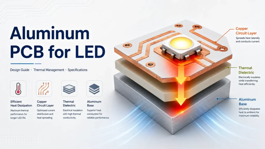
An aluminum PCB for LED products is a metal-base circuit board. Its usual stack has copper circuitry, an insulating dielectric, and an aluminum base. This structure spreads heat away from LED solder pads.
The board does not cool an LED by itself. Heat must pass from the package and solder joint through the board, then reach ambient air. That path may include interface material, a housing, a heat sink, and airflow. Good design starts with the permitted junction temperature and real operating conditions.
What Is an Aluminum PCB and Why Do LEDs Need It?
An aluminum PCB is one type of metal-core printed circuit board, or MCPCB. Other MCPCBs can use different metals. The two terms are related, but they are not always identical.
LEDs convert only part of their electrical input into light. The remaining energy becomes heat. Poor heat removal raises junction temperature. This can affect light output, color stability, and reliability.
The LED datasheet defines the applicable thermal limits. The ams OSRAM LED thermal measurement guide shows how solder-point or board temperature can support a junction-temperature calculation. The method depends on the package and its specified thermal resistance.
An aluminum board can reduce part of the board-level thermal resistance. Suitability still depends on the layout, enclosure, duty cycle, and cooling system.
Aluminum PCB Structure
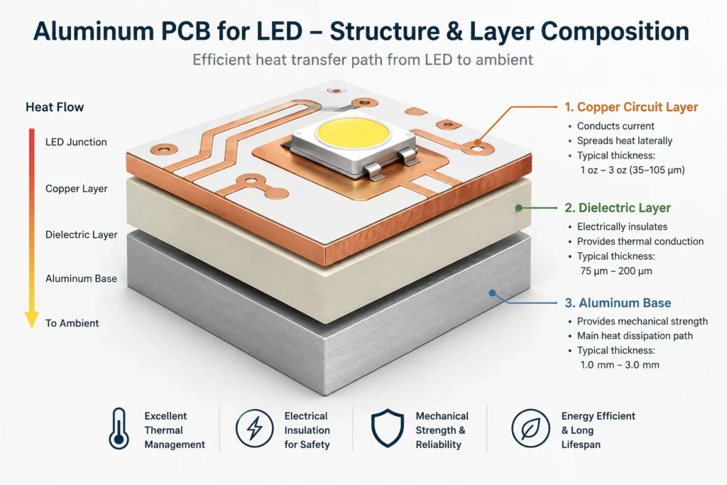
A basic single-sided aluminum PCB has three functional layers. Each layer has a different electrical, mechanical, and thermal role.
Copper circuit layer
The copper layer carries current and spreads heat around thermal pads. Trace width, thickness, pad geometry, and copper area affect electrical loss and local temperature.
Keep high-current paths short where practical. More copper can improve spreading, but it cannot bypass a poor dielectric or heat-sink interface.
Thermally conductive dielectric
The dielectric isolates copper from aluminum and transfers heat through the board. This thin layer often has a strong effect on thermal performance.
Compare conductivity, thickness, tested thermal impedance, dielectric strength, and reliability. A high-conductivity material can still perform poorly if its dielectric is thick.
Aluminum base and external interface
The aluminum base spreads heat and supports the circuit. When the board mounts to a heat sink or housing, heat must cross that interface. Flatness, mounting pressure, and interface material can affect this step.
The aluminum is electrically conductive. Do not assume it is an isolated ground plane. Holes, edges, slots, and exposed metal need defined clearances. Confirm any base connection with the manufacturer.
How to Select Thermal Conductivity for LED Applications
There is no universal conductivity requirement based only on LED wattage. Equal-power boards can reach different temperatures. Efficiency, package resistance, copper area, LED spacing, and airflow all matter.
Start with LED heat, not nameplate power alone. Estimate every resistance from the junction to ambient. Lumileds explains this series path in its practical heat-sink design paper. It includes the PCB, interface material, heat sink, and surrounding air.
Use the table below as a screening guide. It does not assign a universal W/mK value to a power band.
| Power and Layout Context | Main Thermal Risk | Board Information to Compare | Required Check |
|---|---|---|---|
| Lower total power with widely spaced LEDs | Local hot spots near small pads | Dielectric impedance, copper area, board-to-housing interface | Prototype temperature at the specified operating point |
| Moderate power with grouped LEDs | Heat paths overlap between nearby packages | Dielectric stack, copper weight, LED spacing, aluminum thickness | Thermal model plus measurements at center and edge LEDs |
| High power density or compact arrays | The center LED may become the hottest location | Stack impedance, copper geometry, interface material, heat-sink capacity | Worst-case simulation and instrumented prototype testing |
| Any power in a sealed or hot enclosure | Heat accumulates because ambient cooling is limited | Enclosure path, mounting, contact area, airflow, maximum ambient | System test inside the final enclosure |
A Ventec IMS product example shows why thickness matters. Its conductivity stays at 3.0 W/mK across several dielectric options. The listed thermal impedance rises from 0.027 to 0.095 °C·in2/W as thickness increases from 50 to 180 µm. Ventec marks these as typical product values, not universal specifications.
Dielectric Layer Thickness and Thermal Impedance
For a simple layer, resistance rises with thickness and falls with conductivity and area. Real boards also include interfaces, copper coverage, material variation, and spreading effects.
A thinner dielectric can shorten the heat path. It must still meet isolation, dielectric withstand, manufacturing, and reliability requirements. High-voltage strings may need different isolation than low-voltage modules.
Ask for conductivity and thermal impedance data. Confirm the dielectric thickness, test method, and conditions. Values from different test setups may not be comparable.
Model the selected stack, then test production-representative boards. Measure at the LED maker’s recommended point. Use published package resistance where that calculation applies.
Copper Weight Selection for an Aluminum LED PCB
Copper weight should meet electrical and thermal needs. Calculate segment current, voltage drop, trace width, copper temperature rise, and connector limits.
More copper can reduce resistance and improve lateral spreading. It also affects etching, spacing, pad geometry, cost, and soldering. Dense layouts need different tradeoffs than low-current strips.
Review each high-current path. The heavy copper PCB design rules explain why thickness, trace geometry, and manufacturability must be considered together.
Do not copy FR-4 thermal-via rules onto a simple aluminum PCB. Any plated or electrically active feature crossing the conductive base needs a qualified insulated construction.
Aluminum PCB vs Ceramic PCB for High-Power LED
Both board types can manage LED heat, but their paths differ. Aluminum PCB uses a dielectric between copper and metal. Ceramic is itself electrically insulating.
| Design Factor | Aluminum PCB | Ceramic PCB |
|---|---|---|
| Electrical isolation | Depends strongly on the dielectric layer and feature clearances | The ceramic body provides electrical insulation |
| Thermal path | Heat crosses the dielectric before reaching the metal base | Heat crosses the ceramic substrate and its metallization system |
| Mechanical behavior | Metal base supports common LED board shapes | Ceramic is rigid but brittle, so handling and mounting need care |
| Commercial fit | Often cost-effective for common lighting formats and larger panels | May justify higher cost for demanding density or isolation needs |
| Selection method | Compare the complete laminate stack and heat-sink interface | Specify the ceramic type, thickness, metallization, and assembly interface |
Ceramic is not one thermal class. CeramTec’s table lists minimum conductivity values of 24 W/mK for its alumina substrate and 170 W/mK for its AlN substrate. The AlN value is stated at 20°C with the supplier’s measurement tolerance. These values do not apply to every ceramic board.
Aluminum PCB often fits cost-sensitive lighting with a defined heat sink. Ceramic may suit compact power density or high isolation. Use the ceramic PCB vs FR-4 comparison for more material context. Always validate the complete assembly.
Common Aluminum PCB Design Mistakes
- Selecting by W/mK alone. Dielectric thickness, contact area, and interfaces also affect the path.
- Using electrical input as heat. Optical output and operating efficiency affect the estimate. Follow the LED maker’s method.
- Ignoring the package footprint. A poor thermal-pad or land design can restrict heat before it reaches the board.
- Undersizing copper paths. Narrow traces may create voltage drop and additional heating even when the base transfers heat well.
- Ignoring the heat-sink interface. Gaps, weak pressure, unsuitable interface material, or warpage can dominate performance.
- Treating aluminum as an automatic ground. Unplanned contact at holes, edges, or hardware can create insulation and safety risks.
- Skipping center-array measurements. Closely packed LEDs can heat one another. The most accessible LED may not be the hottest one.
- Testing only at room temperature. Enclosure, drive current, duty cycle, ambient, and airflow change the result.
Validate the LED Thermal Path Before Release
- Collect LED data. Record drive conditions, maximum junction temperature, package thermal resistance, and the maker’s sensor-point method.
- Define the environment. Set maximum ambient temperature, enclosure type, airflow, duty cycle, mounting position, and nearby heat sources.
- Build the thermal budget. Include the package, solder joint, board stack, and the applicable housing or heat-sink path to ambient.
- Select a manufacturable stack. Compare dielectric properties, copper weight, aluminum thickness, isolation needs, hole construction, and board geometry.
- Model the worst case. Include component tolerances, material variation, blocked airflow, and the hottest LED in a dense array.
- Measure a representative prototype. Test the final enclosure and operating mode. Compare the estimated junction temperature with the allowed limit.
Document assumptions and measurement locations. If margin is low, change the board, interface, heat sink, drive conditions, or enclosure. Higher laminate conductivity is only one option.
Aluminum PCB for LED FAQ
What thermal conductivity is needed for LED aluminum PCB?
There is no universal value. Select conductivity with dielectric thickness and total impedance. Use the heat load, LED spacing, ambient temperature, heat sink, and junction-temperature limit. Confirm the choice by simulation or prototype testing.
What is the difference between aluminum PCB and ceramic PCB for LED?
An aluminum PCB has copper, a dielectric, and a metal base. A ceramic PCB uses an insulating ceramic substrate with metallization. Ceramic can support demanding thermal or isolation needs. Aluminum PCB often suits larger, cost-sensitive formats. Compare the complete assemblies.
How thick should the dielectric layer be for LED applications?
Use a manufacturable layer that meets isolation and reliability needs. There is no safe universal thickness. Compare conductivity, tested impedance, dielectric withstand, and the approved stack. Validate the board under worst-case conditions.
Can aluminum PCB be used for high-power LED arrays?
Yes, if the full path keeps every LED within its temperature limit. Dense arrays may create a hotter center region. Use simulation, a suitable heat sink, controlled interface material, and representative measurements.
Prepare an Aluminum LED PCB for Review
Share Gerber or ODB++ data, the fabrication drawing, dimensions, quantity, and surface finish. For assembly, also provide the BOM, centroid file, assembly drawing, LED datasheets, and drive conditions.
Include maximum ambient temperature, enclosure details, heat-sink design, interface material, duty cycle, and target margin. State any isolation, thermal-test, or traceability requirements.
Review available LED PCB manufacturing options before release. When the files are ready,
. Request a DFM review of the stack, copper geometry, and thermal interface.

