

EMI Shielding for PCB — Methods and Materials
What Is EMI Shielding on a PCB?
EMI shielding for a PCB uses conductive barriers to reduce unwanted electromagnetic coupling. Metal shield cans isolate circuit blocks. Conductive gaskets close gaps in shielding structures. Ground planes and a suitable stack-up support EMI control, but they do not replace a complete shield.
Choose the method after identifying the noise source, its path, and the affected circuit. Frequency, available space, heat, and cost all matter. A thicker metal cover may achieve little if noise escapes through a seam or cable.
Shielding can help contain emissions or protect sensitive circuits from external interference. It does not, by itself, prove electromagnetic compatibility. The EMI vs EMS vs EMC guide explains those terms and their relationship.
For selection, ask a practical question: does the problem involve one circuit block, an enclosure joint, or a poorly controlled return path? That answer narrows the useful options before you compare materials.
Board-Level Shield Cans and When to Use Them
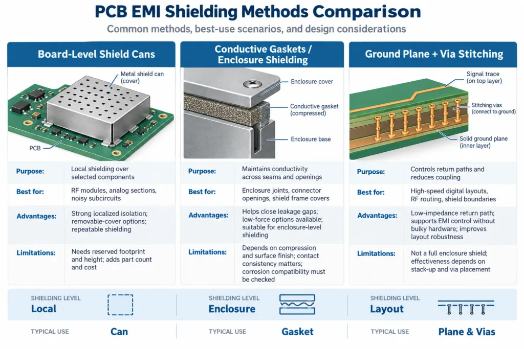
A PCB shield can is a metal cover mounted over selected components. It can separate a noisy circuit from a sensitive receiver or analog section. Reserve its footprint and height early. Adding one after routing may leave insufficient space for reliable mounting.
Laird’s board-level shielding overview distinguishes one-piece cans from two-piece frames with removable covers. A removable lid helps with inspection, testing, and repair. The extra joint and separate part also need mechanical and electrical review.
Plan the shield connection, not just its outline. Würth Elektronik’s shielding guidance emphasizes a low-impedance path to the intended reference. Use the shield supplier’s mounting recommendations. The PCB ground reference is not automatically protective earth.
Before release, check these details with the assembly supplier:
- Ground lands, mounting contacts, and keep-outs match the selected shield.
- Component height and tolerances leave clearance beneath the lid.
- Test points and rework access remain usable.
- Ventilation openings and heat paths are evaluated with the shield installed.
Traces crossing the shield boundary still require attention. A metal lid cannot correct every coupling path through power or signal connections.
Conductive Gaskets and Enclosure-Level Shielding
A conductive gasket connects mating conductive surfaces across a joint. It may sit between enclosure halves, around a connector opening, or between a shield frame and cover. It preserves the electrical path across a seam; it is not a complete enclosure on its own.
Parker’s shielding and gasketing guidance explains why air gaps and poor interface contact allow leakage. A suitable material still needs correct compression and compatible mating surfaces. Paint or an insulating coating at the contact area can interrupt the intended connection.
Fabric-over-foam gaskets can suit joints requiring low closing force. Conductive elastomers are another option where the selected product also provides an environmental seal. Do not assume that every EMI gasket is waterproof. Confirm the required sealing performance separately.
Specify the gap range, compression, mounting method, surface finish, and expected opening cycles. Check corrosion compatibility between the gasket and housing. Mechanical tolerances matter because a joint that works in one prototype may not make consistent contact across production units.
For a complete enclosure, review cable entries and connectors too. Analog Devices’ shielding tutorial explains how interconnects can carry interference across the shielding boundary. Filtering and shield termination must match the interface and frequency. There is no universal rule that every cable shield should connect at only one end.
Ground Plane Design and Via Stitching for EMI Control
A continuous reference plane gives signal return current a nearby path. A gap beneath a critical trace can force that current around a longer route. TI’s high-speed layout guidance recommends organizing circuit blocks while preserving appropriate return paths.
Place noisy and sensitive circuits thoughtfully. Do not split analog and digital grounds simply because their names differ. Follow component guidance and review where current actually flows. Safety isolation boundaries require their own design rules and must not be bridged casually.
Ground stitching vias connect intended ground copper across layers. They can support shield mounting and connect ground regions beside RF traces. When a signal changes between layers referencing connected ground planes, nearby return vias can reduce the return-path detour.
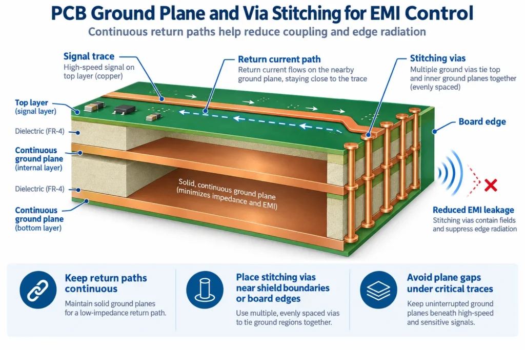
Via placement depends on the frequency content, stack-up, geometry, and required isolation. A fixed via pitch copied from another board is not a universal rule. Ground vias also cannot repair an unrelated break in the return path.
Review clearances around signal vias as well. A dense row of clearance holes can cut a slot through an otherwise solid plane. The guide to PCB stack-up for signal integrity explains how reference layers and routing work together.
Shielding Material Comparison
Choose EMI shielding materials for the actual field, geometry, environment, and assembly process. Conductivity alone does not determine the finished result. Low-frequency magnetic fields may require high-permeability material and a separate design approach.
Tin-Plated Steel
Tin-plated steel is an established option for rigid shield cans. Specify the steel grade, thickness, finish, and soldering requirements. The plating supports the surface connection; the complete can still depends on its seams, mounting, and openings. Do not assume every steel shield handles low-frequency magnetic interference equally.
Copper-Nickel and Nickel Silver
“Copper-nickel” alone is not a complete shielding specification. Confirm the alloy and its intended form. The Copper Development Association classifies nickel silver as a copper-nickel-zinc alloy. It should not be confused with a binary copper-nickel alloy or metal-plated textile. Ask for the exact material designation and finish.
Conductive Fabric
Conductive fabric uses a metal-coated textile and can form a flexible shielding interface. For example, Parker’s SOFT-SHIELD 3700 data sheet describes nickel-plated copper polyester fabric over foam. This construction is not a solid copper-nickel sheet. Check abrasion, compression, temperature, and contact requirements for the selected product.
The comparison below describes application fit, not guaranteed frequency limits. Costs are design-dependent factors, not quotes or fixed rankings. Ground-plane design is included as a complementary control method.
Shielding Method Comparison
| Method | Frequency Range | Cost | Best Use Case |
|---|---|---|---|
| Metal shield can | Target RF bands; verify the assembled can | Shield part, assembly, and possible custom tooling | Isolating one noisy or sensitive circuit block |
| Conductive gasket | Product- and seam-dependent; verify required bands | Gasket, installation, and joint preparation | Maintaining contact across a shielding seam |
| Conductive enclosure | Design-dependent; openings and cable entries matter | Housing, finish, bonding, and sealing | Shielding an electronic assembly as a system |
| Ground plane and via stitching | Signal-spectrum dependent; not a rated enclosure shield | No shield part; layers and routing may affect board cost | Controlling return paths and supporting board-level shielding |
Compare supplier shielding data only when frequency, test method, and mounting conditions are relevant. A material’s laboratory result is not the shielding effectiveness of your finished product.
EMI Shielding for High-Frequency vs Digital Designs
RF designs need attention to the operating band, unwanted harmonics, and sensitive receive paths. Preserve controlled impedance and keep noisy digital routes away from sensitive RF sections. Analog Devices’ RF layout guidance explains the importance of continuous reference planes and signal isolation.
Digital circuits also create high-frequency interference. Fast rise and fall times generate harmonic content well above the clock frequency. Where interface timing allows, slower edges may reduce that energy. A lower clock rate alone does not resolve every emissions problem.
On mixed-signal boards, combine source reduction, controlled return paths, and selective shielding. Use the high frequency PCB design guide for the broader routing and material decisions.
Validate the assembled design in its intended enclosure with representative cables and operating modes. Rohde & Schwarz’s EMI debugging guidance describes using near-field probes to locate interference. Such measurements help compare changes; they do not replace the product’s required compliance tests.
FAQ
What is the most common EMI shielding method for PCBs?
Metal shield cans are a common board-level option for individual circuit blocks. They are not the right answer for every problem. A leaking enclosure seam may need a gasket, while a return-path problem calls for layout changes.
Does a ground plane alone provide sufficient EMI shielding?
Not necessarily. A ground plane supports return-current control but does not enclose the circuit. Depending on the coupling path, the design may also need a shield can, enclosure treatment, filtering, or cable changes.
When should I use a shield can instead of gasket shielding?
Use a can when a particular circuit block needs local shielding. Use a gasket to maintain electrical contact at a joint. They can work together, such as a removable shield cover with a conductive interface.
Does EMI shielding affect PCB manufacturing cost significantly?
It depends on the design and quantity. Added layers or routing constraints affect bare-board fabrication. Shield cans, gaskets, placement, inspection, and enclosure work affect assembly or system cost. Compare these items separately instead of applying a fixed percentage.
Managing EMI in a Compact Design?
Send Benlida your Gerber or ODB++ files, stack-up, fabrication drawing, and proposed shield footprint. Include keep-outs, frequency concerns, quantity, revision, and any existing EMI findings. For assembly inquiries, add the BOM, placement data, and shield-part requirements.
Discuss the fabrication scope through Benlida’s high-frequency PCB manufacturing service. Confirm which manufacturing checks are included and whether electrical analysis or testing needs a separate scope. DFM review alone does not verify shielding effectiveness or EMC compliance.