High Frequency PCB Design Guide — Impedance, Materials & Layout Rules
High frequency PCB design keeps impedance and return current predictable while limiting signal loss, reflection, coupling, and radiation. It starts with the stack-up. The designer must then coordinate dielectric material, trace geometry, reference planes, vias, and component launches.
There is no universal frequency at which every PCB becomes a high frequency design. A 1 GHz RF circuit may need careful transmission-line planning. Path length, structure, bandwidth, allowed loss, and reflection all matter. Fast digital edges can need the same controls at a much lower clock rate.
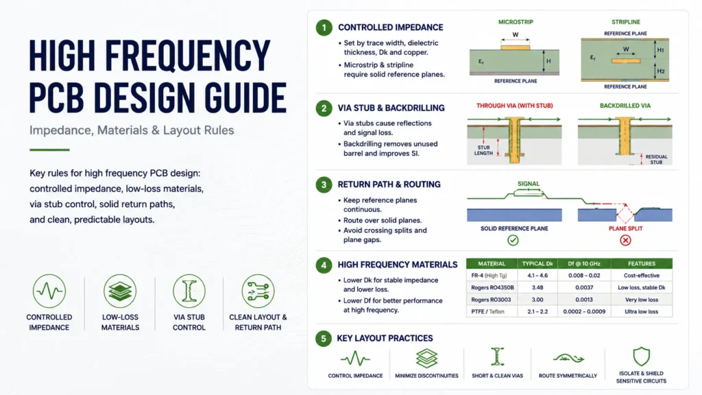
What Makes High Frequency PCB Design Different?
At low frequencies or over very short connections, a trace may behave mainly like a simple conductor. As electrical length increases, the same trace acts as a transmission line. Its characteristic impedance, delay, loss, and return path become part of the circuit.
A high frequency layout therefore cannot be separated from the physical board construction. Trace width alone does not set impedance. Dielectric thickness, copper thickness, copper profile, dielectric constant, solder mask, and nearby copper all change the field around the trace.
The operating frequency is only one input. A wideband pulse contains energy above its repetition or clock frequency. Connector launches, pads, vias, plane gaps, and test points can add discontinuities. The goal is not to remove every discontinuity. It is to keep the remaining effects inside the system’s signal-integrity and RF budgets.
Material Selection for High Frequency PCB
Start material selection with the electrical and environmental requirements. Dielectric constant, or Dk, affects impedance and phase velocity. Dissipation factor, or Df, is one contributor to dielectric loss. Lower Df can help at higher frequencies and over longer routes, but it is not the only selection criterion.
Do not use one generic Dk for every calculation. A data sheet may list process Dk and design Dk from different test methods. Effective Dk also changes with transmission-line structure, thickness, glass reinforcement, copper profile, and frequency. Rogers explains these differences in its guide to PCB materials and controlled impedance.
The following table is a screening aid, not a laminate specification. Frequency alone cannot select a material. Insertion loss, phase stability, temperature, moisture, thermal needs, fabrication route, availability, and cost also matter.
Material starting points for different high frequency PCB design ranges
| Frequency Range (Illustrative) | Recommended Material (Possible Starting Point) | Typical Dk (Supplier Context) | Application (Example) |
|---|---|---|---|
| Below about 1 GHz | A qualified FR-4 grade or low-loss epoxy system when the loss budget allows | No single FR-4 value; use the selected supplier's design data | Mixed-signal control, lower-frequency RF, and short controlled-impedance routes |
| About 1 to 10 GHz | Low-loss hydrocarbon/ceramic laminate; RO4350B is one example | RO4350B average Design Dk: 3.66 from 8 to 40 GHz; verify thickness-specific data | RF front ends, filters, antennas, and wireless infrastructure |
| About 10 to 30 GHz | A validated low-loss microwave laminate chosen from the loss and phase budget | Product- and method-specific; verify the exact construction | Microwave links, radar channels, and phased-array feed networks |
| Above 30 GHz | A tightly controlled mmWave laminate; RO3003 is one possible example | RO3003 process Dk: 3.00 ± 0.04 at 10 GHz; this is not an above-30-GHz Design Dk | Automotive radar, mmWave antennas, and 5G radio modules |
The values above come from product-specific methods. The Rogers RO4000 data sheet lists a process Dk of 3.48 ± 0.05 at 10 GHz. This value applies to RO4350B thicknesses other than 4 mil. It lists 3.33 ± 0.05 for the 4 mil laminate.
The same sheet lists 3.66 as an average Design Dk measured from 8 to 40 GHz. It notes that the value can vary with thickness. The RO3003 product data lists process Dk as 3.00 ± 0.04 and Df as 0.0010 at 10 GHz. These values are examples, not proof that either material fits a specific board.
For a focused material comparison, review the existing Rogers RO4350B material specifications. Then lock the exact laminate code, thickness, copper type, and bonding system before impedance modeling.
Controlled Impedance Design Rules
Characteristic impedance is set by the distributed inductance and capacitance of a transmission line. For a low-loss first estimate, Z0 ≈ √(L′/C′). The geometry and surrounding materials determine both values.
A microstrip runs on an outer layer over a reference plane. Part of its field is in the dielectric and part is in air or coating. A common closed-form estimate is Z0 ≈ 87/√(Dk + 1.41) × ln[5.98h/(0.8w + t)]. Here, h is the dielectric height to the plane, w is trace width, and t is copper thickness.
A symmetric stripline is buried between two reference planes. A common estimate is Z0 ≈ 60/√Dk × ln[1.9b/(0.8w + t)]. Here, b is the spacing between the planes. In both estimates, ln is the natural logarithm. Use the same units for all dimensions.
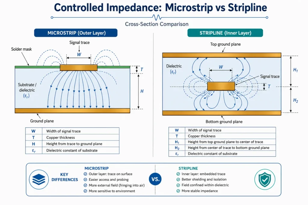
These equations are useful for direction, not final release. They simplify copper shape, roughness, plating, solder mask, resin distribution, and frequency-dependent behavior. Coupled and asymmetric structures need more inputs. Use a suitable 2D or 3D field solver with the proposed stack-up. Then align the model with the fabricator’s finished dimensions and impedance-control method.
Define each controlled net by target impedance, tolerance, layer, reference plane, and routing structure. Include finished copper and the intended dielectric data. Benlida’s PCB stack-up design guide explains the broader layer-planning process. If coupons and TDR results are required, state them in the fabrication drawing and purchase requirements.
Via Stub Effects at High Frequency
A through via can leave unused plated barrel beyond the signal layer. This section is a via stub. Its capacitance and inductance create a discontinuity. A longer stub can resonate at a lower frequency and increase reflection or insertion loss.
Backdrilling removes unwanted copper from the unused part of the barrel. It can reduce stub length without changing the main layer connection. Blind vias, shorter layer transitions, or a different stack-up may solve the same problem.
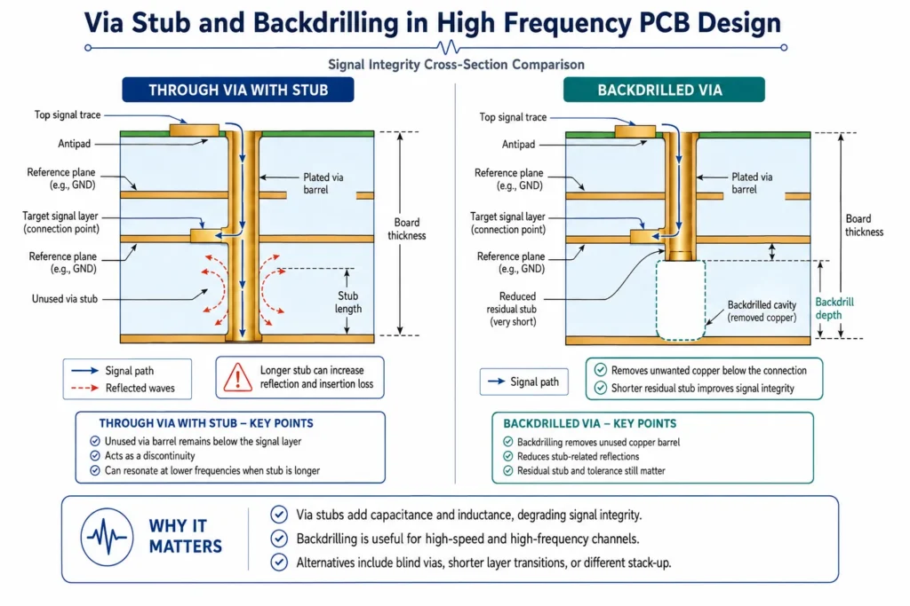
Do not apply one backdrill threshold to every design. The decision depends on the channel bandwidth, stub length, via geometry, antipads, reference transition, residual stub, and manufacturing tolerance. Texas Instruments gives interface-specific examples in its High-Speed Interface Layout Guidelines. Treat those dimensions as guidance for the covered interfaces, not a universal RF rule.
Ground Plane and Return Path Design
High frequency return current follows the path of lowest impedance. Over a continuous reference plane, that path is concentrated near the signal trace. A slot, plane split, or large void forces the current to detour. The larger loop can increase inductance, coupling, radiation, and signal distortion.
Route critical signals over a continuous reference. Keep the same reference when possible. When a signal changes layers, give the return current a nearby path between the relevant planes. This may require a ground stitching via or a properly placed transition capacitor, depending on the reference change.
Analog Devices illustrates why high frequency return current stays close to the trace in its PCB grounding and return-path guide. A differential pair still interacts with reference planes. Do not assume that equal and opposite traces make plane continuity irrelevant.
Trace Routing Rules for High Frequency Signals
- Freeze the stack-up before final routing. Trace width is meaningful only with the dielectric, copper, and reference geometry.
- Keep the impedance environment consistent. Avoid abrupt width changes, large pads, unnecessary test stubs, and unmodeled neck-downs.
- Keep critical routes direct. Extra length adds conductor and dielectric loss. It also creates more opportunities for coupling.
- Control coupling by analysis. Spacing rules depend on layer height, parallel length, edge rate, and the allowed crosstalk. A single spacing multiple is not universal.
- Plan launches and transitions. Connectors, component pads, vias, and packages can dominate a short RF channel. Model them when the budget requires it.
- Use length matching only where the circuit needs it. Match phase-sensitive paths and differential pairs to their real tolerance. Do not add serpentine length without a reason.
- Protect reference continuity. Do not route critical traces across splits or voids. Keep noisy switching nodes away from sensitive RF paths.
Also review copper roughness, solder mask, surface finish, and etch tolerance. Their impact grows as loss budgets tighten. A fabricator can check manufacturability, but the product designer owns the electrical acceptance limits.
Common High Frequency PCB Design Mistakes
- Selecting a laminate from frequency alone, without an insertion-loss, phase, thermal, or cost budget.
- Using a process Dk, design Dk, or generic FR-4 value without checking the test method and construction.
- Routing controlled traces before the stack-up and finished copper are defined.
- Checking trace impedance while ignoring pads, vias, connectors, plane changes, and return paths.
- Using a simple closed-form equation as final proof for a complex or coupled structure.
- Adding backdrilling without defining the drill side, target layer, residual stub, diameter, and tolerance.
- Copying one spacing, length-matching, or grounding rule into every RF and high-speed interface.
A useful design release connects each rule to a requirement. State target impedance, tolerance, operating band, loss limit, phase or skew limit, reference planes, via transitions, material construction, and verification method. This makes the layout easier to review and the fabrication package easier to quote.
High Frequency PCB Design FAQ
What dielectric constant is best for a high frequency PCB?
There is no universal best Dk. Lower Dk can support wider traces for a given impedance and may help some antenna or low-capacitance structures. Other designs need a higher Dk for size reduction. Select a stable, well-characterized value that fits the loss, geometry, phase, thermal, and fabrication requirements.
What is a via stub, and why does it matter at high frequency?
A via stub is unused plated barrel beyond the signal’s connection layer. It adds parasitic capacitance and inductance. A long stub can resonate, increase insertion loss, and cause reflection. Review the complete via model rather than judging only the drilled length.
When should backdrilling be used?
Use backdrilling when analysis shows that an unused via stub threatens the channel budget. The fabricator must also hold the required residual stub. Compare backdrilling with shorter transitions, blind vias, and stack-up changes. State the drill side, depth, diameter, target layer, and tolerance.
What is the difference between microstrip and stripline?
Microstrip is an outer-layer trace referenced to a plane. Its field spans the board dielectric and the material above the trace. Stripline is buried between reference planes and is surrounded mainly by dielectric. Stripline offers stronger field containment, while microstrip is easier to access and inspect.
What frequency range requires special PCB design considerations?
No single frequency sets the boundary. RF boards often need transmission-line controls around 1 GHz and above, but fast digital edges can require them at lower clock rates. Compare interconnect delay with rise time. Also review bandwidth, route length, loss, and the allowed reflection or crosstalk.
Prepare Your High Frequency PCB for Review
Share the operating band, stack-up, laminate construction, target impedance and tolerance, copper type, critical routes, via transitions, and acceptance method. Include Gerber or ODB++, NC Drill, fabrication drawings, and any impedance coupon or test requirements.
Review Benlida’s high frequency PCB manufacturing page for the public service overview. For project-specific questions, request an RF PCB design review. Final material availability, build rules, tolerances, and test coverage still need confirmation for the exact project.

