PCB Impedance Control — What It Is and How to Specify It Correctly
PCB impedance control means matching selected traces to an agreed impedance. Common examples are 50 ohms single-ended and 100 ohms differential. These are not universal defaults. The correct target comes from the interface, device, RF network, or channel specification.
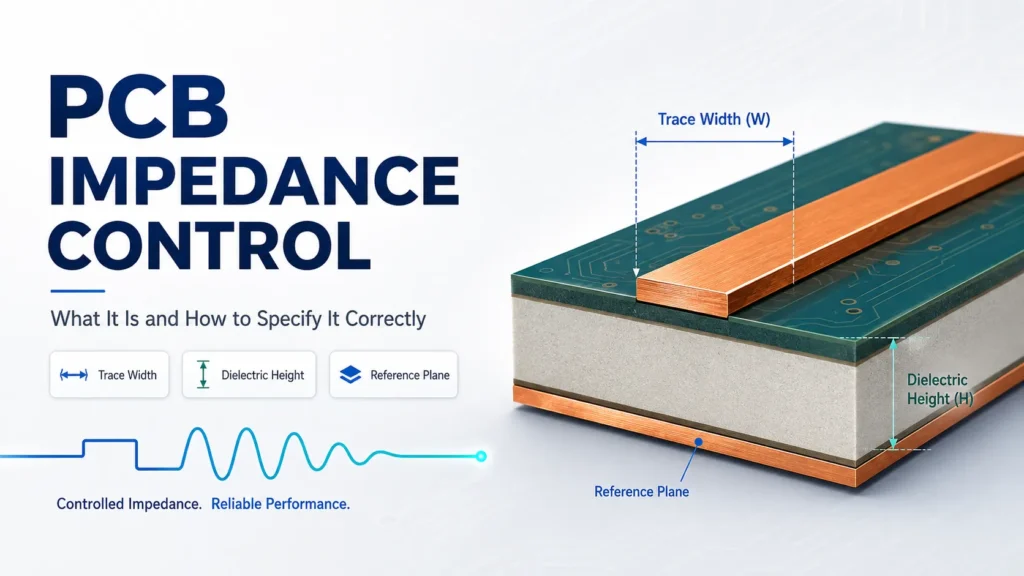
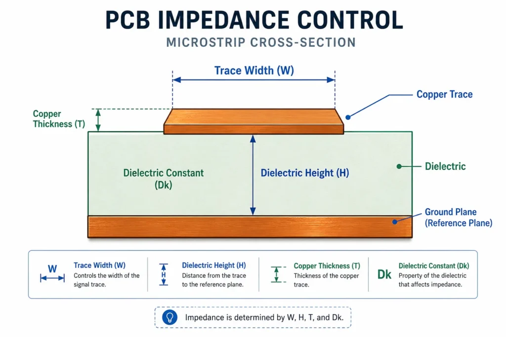
Trace width alone does not set impedance. Finished copper thickness, spacing, dielectric height, material Dk, reference planes, solder mask, and process variation also matter. For an RFQ, identify each single-ended or differential structure, target, tolerance, layer, reference plane, approved stack-up, adjustment rules, coupon, test method, and report requirements.
What Is PCB Impedance Control?
A PCB trace behaves like a transmission line when its electrical length is significant compared with the signal edge. That line has a characteristic impedance. The value comes from distributed inductance and capacitance along the trace.
Characteristic impedance is not DC resistance. A multimeter cannot verify a 50-ohm transmission line.
PCB impedance control coordinates the layout, stack-up, material data, fabrication process, and testing. The designer defines the electrical requirement. The PCB manufacturer then builds the approved geometry within agreed process limits.
Keeping a trace near its target impedance helps reduce reflections caused by impedance discontinuities. Reflection at a transition depends on the impedance difference between the adjoining structures.
Impedance control does not remove all signal loss. Conductor resistance, copper roughness, dielectric loss, vias, connectors, and crosstalk can still affect the channel.
Controlled impedance is also not the same as a fully impedance-matched system. The transmitter, receiver, termination, connector, cable, and PCB path must work together. Differential impedance also depends on coupling between the two traces. Two separate 50-ohm traces do not automatically create a 100-ohm differential pair.
When Do You Need Controlled Impedance?
Controlled impedance is usually considered when a routed interconnect behaves as a transmission line. Clock frequency alone cannot make that decision. Edge rise time, propagation delay, route length, loading, and allowed reflection all matter.
Analog Devices provides a practical starting rule in its high-speed logic transmission-line guide. It compares one-way trace delay with signal rise or fall time. The applicable device and interface documentation should still control the final design.
Common use cases include high-speed serial links, fast clocks, memory buses, RF paths, antennas, and links to controlled-impedance connectors or cables. USB, HDMI, Ethernet, and similar interfaces can require differential impedance. Their target values and tolerances depend on the applicable specification and implementation.
A slow or very short route may not need a formal impedance-control requirement. It still needs a continuous return path and suitable layout. Review the full high frequency PCB design context before removing a controlled structure from the fabrication notes.
Factors That Determine PCB Impedance
Characteristic impedance is a property of a complete transmission-line cross-section. Use the proposed production stack-up when calculating it. Generic online values can be useful for direction, but they are not release data.
Trace geometry and finished copper
Trace width and finished copper thickness affect impedance. So do the etched sidewall shape and local copper distribution. Copper weight is only a starting description. Plating can change the finished geometry from the value used in the layout.
Differential pairs add another variable: spacing. A change in width or spacing changes coupling and differential impedance. Keep the pair geometry consistent through the controlled region. Pads, neck-downs, vias, and connectors create local transitions that need separate review.
Dielectric construction and reference planes
The distance from a trace to its reference plane has a strong effect on impedance. Material permittivity, often called Dk, also matters. Dk can vary with resin content, glass style, test method, and frequency.
Use supplier data that matches the selected laminate construction and calculation method. Do not use one generic FR-4 Dk for every layer. The PCB stack-up design should identify signal layers, reference planes, dielectric thicknesses, and material constraints.
Reference planes should remain continuous below or around the controlled route. Splits, voids, anti-pads, and layer changes can disturb the return path. They may create a local discontinuity even when the straight trace meets its target.
Solder mask, roughness, and process variation
Solder mask can change the effective dielectric around an outer-layer trace. Its effect depends on the structure and coating. Copper roughness becomes more important as frequency and loss sensitivity increase.
Pressed dielectric thickness, etching, plating, and material variation change the finished board. A field solver can model the proposed cross-section with fabricator data. Polar Instruments explains why field-solving methods and representative coupons are used for controlled-impedance production.
How to Specify Impedance to Your PCB Manufacturer
Start with the electrical requirement, not a preferred trace width. The interface or system owner should define the target and acceptable tolerance. Then coordinate the layout and stack-up with the selected manufacturer.
Gerber files alone may not communicate every requirement. Add a clear impedance table and fabrication notes. Identify the controlled nets or net classes in a format both teams can use.
| Specification Field | What to State | Why It Matters |
|---|---|---|
| Controlled structure. | Single-ended or differential, target impedance, tolerance, and net class. | Separates each electrical requirement. |
| Layer and reference. | Routing layer, microstrip or stripline structure, and reference plane or planes. | Defines the field geometry and return path. |
| Nominal geometry. | Trace width, differential spacing, finished copper, and permitted adjustments. | Connects layout constraints with fabrication control. |
| Material stack-up. | Laminate construction, dielectric thickness, Dk basis, and solder-mask condition. | Provides the inputs used by the field solver. |
| Verification. | TDR method, coupon structures, sampling plan, report, and acceptance limits. | Defines how compliance will be judged. |
Ask whether the manufacturer needs to adjust nominal width or spacing for its qualified materials and process. Define the allowed change before fabrication. Request an updated stack-up or impedance drawing when geometry changes.
A useful release package includes Gerber or ODB++, NC Drill data, the fabrication drawing, stack-up, and impedance table. Add material constraints, total thickness, finished copper, solder-mask requirements, and any coupon or report requirement.
Impedance Tolerance and TDR Testing
A 10 percent tolerance is a common starting point, but it is not a universal rule. For example, 50 ohms at plus or minus 10 percent allows 45 to 55 ohms. The interface owner must confirm whether that range is acceptable.
Tighter limits can require more material control, geometry margin, testing, and communication. They can also affect manufacturability, yield, and cost. Do not request plus or minus 5 percent only because it appears more precise.
Time-domain reflectometry, or TDR, launches a fast edge into a transmission line and measures the reflected response. Keysight describes how TDR locates impedance discontinuities and converts the response into impedance versus time or distance.
PCB manufacturers often test a coupon built on the same panel. The coupon should represent the controlled layer, reference plane, dielectric, copper, trace geometry, and coating condition. It supports process verification without probing every functional route.
IPC publishes IPC-TM-650 Method 2.5.5.7A for characteristic-impedance measurement by TDR. The method does not supply one universal target or tolerance. Those remain contractual design inputs.
A coupon result cannot prove the full channel. Actual vias, connectors, packages, plane gaps, and routing transitions may add discontinuities. TDR impedance testing also does not replace insertion-loss analysis, continuity testing, or functional validation.
Common Impedance Control Mistakes
- Using 50 or 100 ohms by habit. Confirm the target in the applicable interface, device, or channel specification.
- Routing before the stack-up is stable. Later dielectric changes can force wider or narrower traces and new spacing.
- Specifying only trace width. Reference planes, dielectric height, Dk, copper thickness, and spacing are part of the structure.
- Ignoring finished geometry. Plating and etching can change the copper cross-section used by the field solver.
- Treating two traces as a differential pair automatically. Differential impedance depends on coupling, symmetry, and spacing.
- Routing across a plane split. A broken return path can create a serious discontinuity and more emissions.
- Leaving tolerance or testing undefined. The manufacturer needs a measurable acceptance rule before production.
- Assuming a passing coupon proves the channel. Review vias, launches, connectors, packages, and other local transitions separately.
PCB Impedance Control FAQ
What is the standard impedance value for single-ended traces?
There is no universal value for every PCB trace. A 50-ohm single-ended target is common in many RF and high-speed systems. Other interfaces use different values. Follow the relevant device, interface, connector, cable, or channel specification.
How is PCB impedance tested and verified?
Manufacturers commonly use TDR on a representative test coupon. The measured profile is compared with the agreed target and tolerance. The result verifies the fabricated coupon structure against the agreed limits and provides representative evidence of process control. It does not prove every discontinuity in the assembled channel.
What information do I need to provide for impedance control?
Provide the target, tolerance, single-ended or differential structure, controlled nets, routing layer, and reference plane. Also provide the stack-up, material constraints, finished copper, nominal width and spacing, solder-mask condition, and test or report requirements.
What tolerance is typical for controlled impedance PCB?
Plus or minus 10 percent is a common starting tolerance, but it is not universal. Some channels require tighter or asymmetric limits. Use the applicable interface and system budget. Confirm that the manufacturer accepts the tolerance and test method before release.
Prepare Your Controlled-Impedance PCB for Review
Share the interface requirements, Gerber or ODB++, NC Drill files, stack-up, fabrication drawing, impedance table, and material constraints. Include the board quantity and any coupon, sampling, or test-report requirements.
Review available high frequency PCB manufacturing information before freezing the stack-up. When the production package is ready,
and ask for a project-specific DFM review.

