

5G PCB Design — Material Requirements and Design Rules
What Makes 5G PCB Design Different?
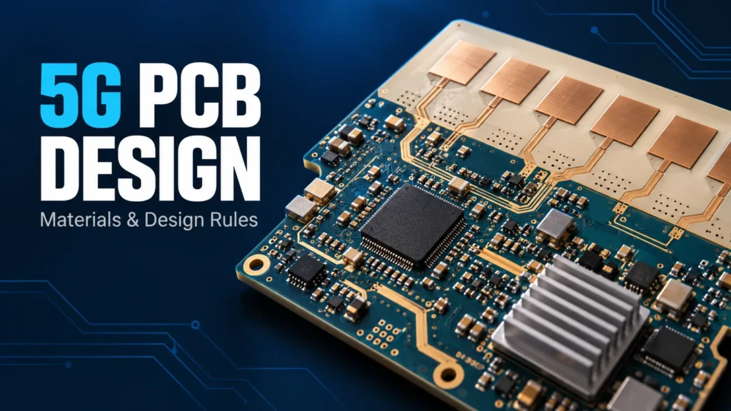
5G PCB design starts with the operating band and the board’s role. RF paths may need low-loss materials, controlled impedance, and stable phase response. Power and control circuits have different priorities. For mmWave designs, short wavelengths make small layout and manufacturing changes more significant. Material selection, antenna design, and heat removal therefore need early coordination.
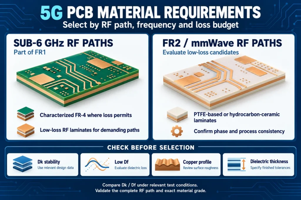
Not every 5G product uses millimeter-wave frequencies. In 3GPP’s NR base-station specification published by ETSI, FR1 spans 410 MHz to 7.125 GHz. FR2 includes 24.25–52.6 GHz and 52.6–71 GHz ranges. These are range definitions, not a list of bands available in every market. “Sub-6 GHz” describes only part of FR1.
A board carrying a ready-made radio module also differs from a board carrying antenna elements and exposed RF feeds. Identify which signals actually travel through the PCB before choosing its material. The 5G label alone does not define a stack-up.
Low-Loss Material Requirements for Sub-6GHz vs mmWave
Useful 5G PCB material requirements describe electrical performance, construction, and operating conditions. Dielectric constant, or Dk, affects wave propagation and transmission-line geometry. Dissipation factor (Df), also called loss tangent, describes dielectric loss. A lower Df can help reduce dielectric loss, but it does not describe the complete circuit loss.
The table gives starting points for an engineering shortlist. Each material family still needs validation against the actual signal path and manufacturing process.
5G Frequency Band Material
| Frequency Band | Recommended Material | Key Constraint |
|---|---|---|
| Sub-6 GHz RF paths within FR1 | Characterized FR-4 where loss permits; RF thermoset laminate for more demanding paths. | Feed length, loss allowance, phase stability, and antenna requirements. |
| Upper FR1 above 6 GHz to 7.125 GHz | Evaluate low-loss RF laminates using data relevant to the operating band. | No automatic material change at 6 GHz; validate the complete channel. |
| FR2 mmWave paths, including 28 GHz and 39 GHz examples | Evaluate low-loss PTFE-based or hydrocarbon-ceramic RF laminates. | Copper roughness, dielectric thickness, transitions, and phase consistency. |
FR-4 is a broad material category, not a complete RF specification. Compare actual grades rather than generic names. Our high frequency PCB materials comparison introduces common options. The Rogers RO4350B PCB material guide provides context for one candidate, not a universal 5G requirement.
Compare dielectric data at compatible frequencies, temperatures, and conditioning, with the test method identified. Rogers’ explanation of specification and design Dk shows why different methods can produce different values. Ask which value fits your transmission-line model. Also review moisture response, temperature stability, copper foil, and finished dielectric thickness.
A low-loss laminate for 5G should be selected against a loss budget: the signal loss that the system can tolerate. Rogers’ material-selection discussion considers frequency alongside power, size, and other application needs. A short route and a long antenna feed may justify different choices. Specify the exact grade and approved alternatives. A substitution with a similar nominal Dk still needs an RF review.
Impedance Control at 5G Frequencies
Consistent impedance and well-matched transitions help reduce reflections along an RF connection. Many RF interfaces use 50 ohms, but the device and circuit requirements determine the target. Do not assign the same value to every signal merely because the product supports 5G.
Trace width alone does not set impedance. Dielectric thickness, Dk, copper thickness, and nearby ground geometry also matter. Analog Devices’ beamformer PCB guidance explains why connector transitions and manufacturing variation need attention alongside the transmission line.
For a practical review:
- Agree on the material construction and finished layer thicknesses before final routing.
- Choose microstrip, stripline, or grounded coplanar waveguide to suit routing and isolation needs.
- Keep the intended reference plane continuous along each RF transmission line.
- Model connector launches, component pads, and layer changes as parts of the RF path.
- Check the permitted manufacturing variation, not just the nominal geometry.
Use the PCB impedance control guide when preparing fabrication notes. State the target, tolerance, relevant nets, and test method. An impedance coupon can check a representative structure. It does not establish antenna efficiency or prove that every transition meets the RF requirements.
Plan RF measurements before ordering prototypes. Define the reference planes and fixture treatment for insertion-loss and reflection measurements. Otherwise, connector or fixture behavior may be mistaken for a laminate problem.
Thermal Management for 5G RF Components
Power amplifiers, beamformer ICs, and power converters can create concentrated heat sources. Their dissipation, duty cycle, and surroundings determine cooling needs. Operating frequency alone does not tell you how hot a board will run.
Map heat from each important device through its package, PCB, interface materials, and enclosure. Select copper planes, thermal vias, spreaders, or heat sinks as part of that path. Follow the component’s thermal-pad and assembly guidance. A low-loss dielectric is not automatically an effective heat spreader.
Texas Instruments’ antenna-on-package thermal guide illustrates how package geometry can restrict cooling options. Its example is a mmWave radar sensor, not a general 5G stack-up. The useful lesson is to check whether a proposed heat sink or copper feature interferes with the antenna.
Thermal vias and RF grounding vias serve different purposes, even when some structures support both. Place them where the package and antenna design allow. More copper or more vias everywhere is not a reliable design rule.
Check expected ambient temperature, enclosure airflow, and the highest sustained operating load. Validate temperatures on the assembled prototype. Keep thermal changes under RF review because nearby metal and geometry changes can affect antenna behavior.
Stack-Up Considerations for 5G Antenna Modules
Start with the antenna architecture and RF component placement. A PCB antenna array, an antenna-in-package device, and a connector-fed external antenna impose different stack-up requirements. There is no fixed layer count for all 5G antenna modules.
Assign layers for antenna structures, RF feeds, reference planes, power, and control routing. A hybrid construction can put suitable RF material around critical paths while using other materials for less demanding circuitry. The fabricator must confirm the bonding system, processing compatibility, and finished dimensions.
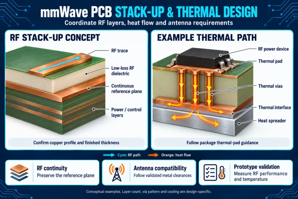
Rogers’ mmWave fabrication guidance explains how copper roughness affects both loss and phase. Include the foil construction in the specification. Also model solder mask and surface finish where they interact with exposed RF structures.
Do not assume that the thinnest dielectric gives the lowest total loss. Thickness changes trace geometry and the balance of conductor and dielectric losses. Evaluate the chosen structure as a whole.
For arrays, review electrical path consistency between channels, including transitions. Equal physical trace lengths do not guarantee equal phase through different structures. Antenna ground and keepout requirements are also architecture-specific. A patch antenna may require a defined ground plane; another antenna may require a copper-free region. Follow the validated antenna design.
Common 5G PCB Design Challenges
A recurring challenge in 5G RF PCB layout is fitting many channels near a compact device. Closely spaced parallel routes can couple energy into each other. Analog Devices’ channel-isolation guidance shows why frequency, spacing, parallel length, and line structure must be evaluated together.
Buried routing can improve isolation in suitable designs, but it adds transitions back to surface-mounted components. Ground-via arrangements need simulation and validation. A copied via-fence pitch is not a substitute for checking your own geometry and band.
Manufacturing changes are another risk. An apparently minor adjustment to dielectric thickness, copper treatment, or finish may change RF behavior. Put critical requirements on the fabrication drawing and require approval before substitutions.
Consider a purchasing example. Two quotations may name the same laminate family but use different copper foils or bonding materials. Treat them as different proposed constructions until the engineering team confirms equivalence. Keep the approved stack-up with the order so purchasing and production use the same specification.
Before release, check that the manufacturing package answers these questions:
- Which operating bands and RF paths determine the material choice?
- What are the agreed stack-up, copper construction, and finished dimensions?
- Which impedance, loss, isolation, and phase requirements need measurement?
- Who owns antenna validation, thermal testing, and acceptance of substitutions?
- Are the Gerber or ODB++ files, drill data, drawings, and revision identifiers consistent?
Separate bare-board fabrication checks from assembled radio testing. Electrical continuity and dimensional inspection do not establish RF system compliance. Agree on test responsibility before placing the order.
Keep prototype results tied to the tested revision. Record the actual material construction, fixtures, operating conditions, and accepted deviations. If the production stack-up changes, decide which measurements need repeating. This makes the prototype a useful reference instead of an approval that silently covers a different board.
FAQ
Do 5G PCBs require different materials than 4G designs?
Sometimes, but not because of the generation name alone. Compare operating frequency, path length, power, loss allowance, and antenna requirements. Some sub-6 GHz designs can use an already qualified material. Moving to mmWave usually demands closer attention to dielectric behavior, copper construction, and manufacturing consistency.
What loss tangent is acceptable for mmWave PCB design?
There is no single acceptable loss tangent for every mmWave PCB. Choose a candidate using dielectric data relevant to the operating frequency and test method. Then calculate and measure the complete path loss. Copper, connectors, transitions, and radiation can consume the budget even when the dielectric loss is low.
Does 5G PCB design require special thermal management?
It depends on the components and operating conditions. Dense RF circuitry may need a deliberately engineered heat path. Follow package guidance, evaluate sustained power and ambient conditions, and verify the assembled design. Cooling structures must remain compatible with antenna placement and RF performance.
Can Benlida manufacture PCBs for 5G antenna modules?
Suitability needs confirmation for the specific design. Use Benlida’s high-frequency PCB service information as a starting point. Submit the operating band, material specification, stack-up, RF requirements, and design files. Ask the team to confirm material availability, fabrication tolerances, and the agreed inspection scope before committing to production.
Designing for 5G or mmWave?
Discuss your 5G PCB project with Benlida using the actual RF and manufacturing requirements. Send Gerber or ODB++ files, drill data, the fabrication drawing, proposed stack-up, quantity, and revision. For assembly, include the BOM, placement data, and test requirements.
Request confirmation of the material, process limits, and review scope for your design. Keep RF simulation and antenna qualification responsibilities explicit. A manufacturing review should support, not replace, system-level validation.