PCB Thermal Management — Design Guide for Heat Dissipation
PCB thermal management controls component temperatures by moving heat through copper, thermal vias, board materials, and cooling interfaces. The heat must eventually reach the surrounding air, a chassis, or another cooling system. Adding copper or changing the substrate helps only when it improves that complete path.
Start with the heat generated by each component, its permitted temperature, and the operating environment. Then design the board and mechanical assembly together. This approach helps reduce overheating risk without assuming that a particular material or via pattern guarantees reliable operation.
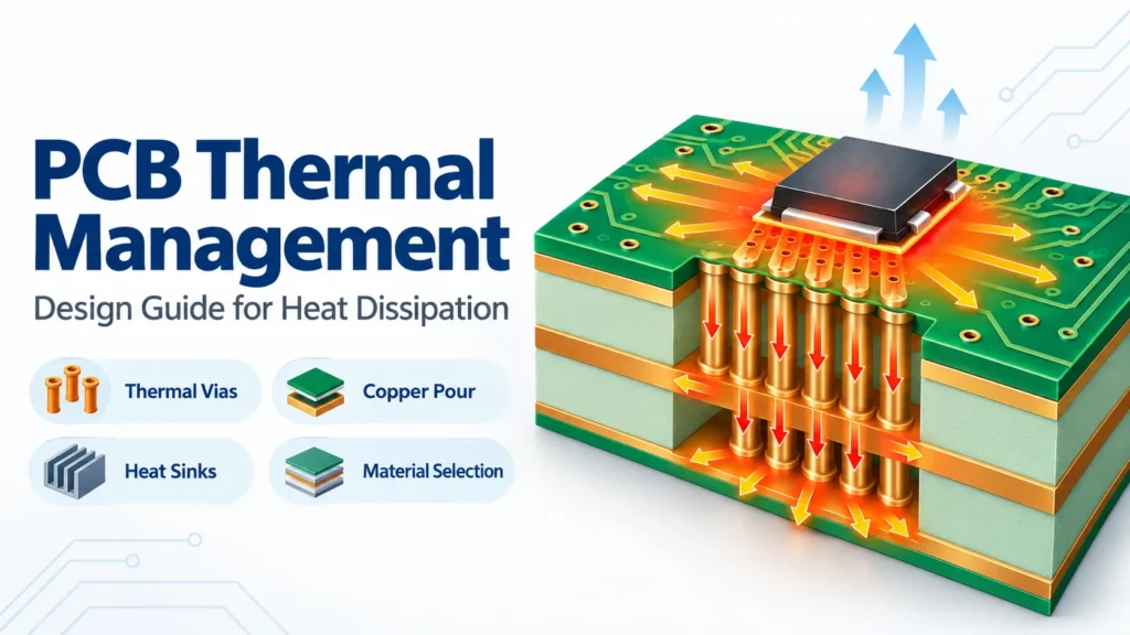
Why PCB Thermal Management Matters
High temperatures can affect component performance and reliability. The hottest device may also heat nearby capacitors, connectors, or sensors. An acceptable average board temperature can hide a local hotspot.
Estimate the power each component dissipates as heat, not simply the product’s input or output power. Include expected load changes and nearby heat sources. Define the local ambient temperature inside the enclosure, rather than relying only on room temperature.
Thermal resistance describes the temperature rise per watt along a specified heat path. Lower resistance means a smaller rise under the same conditions. However, a data-sheet junction-to-ambient value, often written as RθJA, depends on the test board and environment. TI’s explanation of thermal metrics shows why actual PCB layout matters.
Set temperature limits before routing. Distinguish semiconductor junction temperature from package-surface, board, and ambient temperatures. They are different measurement points, not interchangeable readings.
For a hypothetical steady-state example, a device dissipates 2 W and has a 40°C allowable junction-to-ambient temperature rise. Its effective junction-to-ambient thermal resistance must therefore be 20°C/W or lower. This is a design target, not a measured board result. Check transient loading and neighboring heat sources separately when building the model.
Thermal Via Design
Thermal vias provide a conductive path through the board. Their plated copper walls connect a hot component’s land area to internal planes or backside copper. This helps heat spread beyond the small mounting pad.
Place the array where it connects the package’s intended heat-transfer surface to useful copper. Confirm the exposed pad’s electrical connection in the device data sheet. It may require a specific net; it must not automatically be connected to ground.
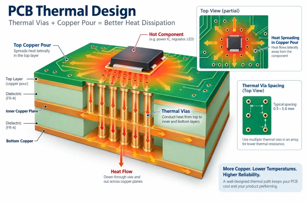
Choose Via Spacing from the Package Guidance
There is no universal thermal via spacing rule. Pad size, board thickness, hole size, copper plating, and assembly requirements all affect the design. Pitch means the center-to-center distance between neighboring vias, not the gap between their edges.
For example, Analog Devices’ LFCSP design guide describes a 7 × 7 mm, 48-lead package example. It recommends via diameters of 0.3–0.33 mm with a pitch of 1.0–1.2 mm. These are package-guide values, not a general PCB rule. Check the current instructions for your exact device before using them.
More vias can reduce the array’s thermal resistance, but the benefit eventually becomes smaller. Extra holes offer limited value when another part of the heat path dominates. Confirm drill and finished-hole dimensions with the fabricator instead of treating them as the same dimension.
Coordinate Via-in-Pad with Assembly
A via-in-pad sits within a component’s solderable land. An open hole can draw solder away from the joint during reflow. TI’s PowerPAD application report discusses how thermal via design affects both heat transfer and solder attachment.
Specify the hole treatment, surface condition, and solder-paste pattern together. Filling and copper capping may be appropriate, but they are not mandatory for every package. A resin-filled via is also not the same as a solid copper-filled via. Ask the fabricator and assembler to review the proposed structure before release.
Copper Pour and Plane Design for Heat Dissipation
A copper pour is a filled copper area on a routing layer. A plane is a more extensive copper layer or region. Both can spread heat away from a component when their connections form a useful thermal path.
Focus on continuity, not just total copper area. A large pour connected through a narrow neck can still restrict heat flow. Slots, cutouts, and routing channels may separate the hotspot from the copper intended to cool it.
TI’s PCB thermal design guidance explains the effect of breaks in a copper heat-spreading path. Review the route from the component pad to the spreading area on each relevant layer. A connection visible in the layout may still be too narrow to work well thermally.
Thermal reliefs need separate attention. Their narrow spokes make pads easier to solder by limiting heat flow into a plane. That purpose differs from a thermal via, which is intended to transfer heat. Follow package guidance for exposed-pad connections and coordinate solid connections with the soldering process.
Electrical design still governs where copper can go. Maintain required isolation and signal return paths. Do not enlarge a switching-node pour solely for cooling, because its size can affect noise coupling. Use the approved electrical net and seek heat-spreading area where it does not compromise circuit behavior.
Material Selection for Thermal Management
Compare the full stackup, not a single thermal-conductivity figure. Dielectric thickness, copper arrangement, heat-source area, and attachment layers all affect heat flow. A high glass-transition temperature, or Tg, does not by itself mean high thermal conductivity.
FR-4 designs can use copper planes and vias to route heat around the relatively resistive laminate. In a conventional metal-core PCB, an insulating dielectric separates the circuit copper from the metal base. That dielectric can be a major part of the thermal resistance, as shown in Cree LED’s PCB thermal performance guide. Our aluminum PCB thermal design guide covers this structure in more detail.
Ceramic offers another combination of insulation and heat transfer. However, alumina, aluminum nitride, and silicon nitride are different materials. Rogers’ ceramic substrate range illustrates different thermal and mechanical priorities. Review ceramic PCB for thermal applications when the available space, isolation, or operating conditions justify evaluating this option.
Confirm the exact material grade and construction. Changing the substrate can also change routing options, mounting methods, assembly processes, and cost.
Heavy Copper for Thermal Design
Thicker copper can spread heat laterally and reduce DC resistance in a current path. For a constant current, lower resistance reduces resistive heating. This relationship is commonly written as P = I²R, where P is heat-producing electrical loss. Switching and high-frequency losses need separate analysis.
Width, thickness, and path length must be considered together. TI’s high-current power-supply layout discussion explains these connections. Check neckdowns, pad entries, connectors, and layer transitions as well as the wide copper sections. A short bottleneck can remain hot after the rest of the plane is enlarged.
Heavy copper is useful when the current and temperature-rise analysis supports it. It cannot correct poor contact with a heat sink or inadequate airflow. There is no single circuit wattage that makes heavy copper mandatory.
Before increasing copper weight, discuss trace geometry, spacing, stackup, and soldering needs. Greater thermal mass can change assembly heating requirements. Our heavy copper PCB design guide explains the broader manufacturing tradeoffs.
Heat Sink Integration with PCB Design
A heat sink works only when heat can reach it and then leave it. Plan its location, contact surface, mounting holes, and enclosure clearance early. Check the component’s preferred heat path before choosing a top-mounted or board-mounted arrangement.
A thermal interface material, or TIM, reduces air gaps between mating surfaces. Cree LED’s thermal management guide explains why thickness and interface properties matter alongside thermal conductivity. Select the TIM for the actual gap, electrical isolation, temperature range, and service conditions.
Review flatness, mounting pressure, and mechanical support. Excessive board bending can stress components and solder joints. A thicker pad may bridge a larger gap, but it can also add thermal resistance. Follow the interface supplier’s installation guidance rather than assuming that more material improves cooling.
Validate the assembled product under representative conditions:
- Use the intended enclosure, mounting orientation, airflow, and nearby heat sources.
- Test the demanding operating loads, including relevant startup or transient conditions.
- Measure identified hotspots and record where each temperature was taken.
- Compare results with the specified limits and investigate any disagreement with the thermal model.
A surface measurement does not directly reveal the semiconductor junction temperature. Use the device supplier’s recommended estimation or measurement method. Document the final board revision, interface material, mounting arrangement, and test conditions so later builds can be compared consistently.
FAQ
How do thermal vias improve heat dissipation?
Thermal vias conduct heat through their copper walls to other board layers or backside copper. They help the heat reach a larger spreading area or cooling interface. Performance depends on the array, copper connections, and complete heat path. Adding vias alone does not guarantee a lower operating temperature.
What copper pour design improves thermal performance?
Use well-connected copper around the heat source and preserve broad paths toward useful spreading areas. Avoid unnecessary neckdowns and breaks. Check connections on internal layers as well as the surface. Balance thermal goals with solderability, electrical isolation, current loops, and switching-node noise requirements.
When is heavy copper needed for thermal management?
Consider heavy copper when current-path resistance or limited lateral heat spreading prevents the design from meeting its temperature-rise target. Compare thicker copper with wider conductors, additional connected layers, and changes to cooling. The decision needs a project-specific analysis, not a universal power threshold.
Does PCB material choice affect thermal performance?
Yes. The substrate and dielectric layers influence how heat travels through the board. Their thickness and material properties matter, but so do copper geometry, vias, solder attachment, and external cooling. Compare complete structures under the same operating conditions before selecting FR-4, a metal-core PCB, or ceramic.
Discuss Your PCB Thermal Design with Benlida
Prepare your Gerber or ODB++ files, stackup, fabrication drawing, and revision details. Add a component heat map or loss estimates, temperature limits, and cooling requirements. For assembly, include the BOM, placement data, and mechanical drawings.
Mark critical thermal features on the fabrication and assembly drawings. Identify required copper layers, via treatment, contact areas, and any keepouts. This gives the supplier a clear record of features that should not change during manufacturing review.
Ask Benlida about a thermal design review and confirm the available scope. State which decisions need review, such as via processing, copper weight, or material selection.

