

PCB Fabrication Process — Step by Step
What Is the PCB Fabrication Process?
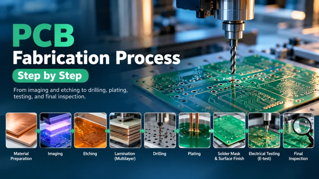
The PCB fabrication process turns copper-clad materials into a finished bare circuit board. For a common multilayer board, it starts with inner-layer imaging and etching, followed by lamination. Drilling, hole metallization, and outer-layer circuit formation come next. Solder mask, identification markings, surface finishing, and final checks complete the board.
Fabrication creates copper connections and the structure that supports them. Assembly adds components and solder joints. Our guide to the PCB assembly process step by step explains that separate stage.
Before production, the fabricator reviews manufacturing files, materials, dimensions, and the proposed layer stack. This review should resolve conflicting revisions, unclear hole definitions, and missing requirements. It cannot establish that the circuit design will perform its intended function.
Keep one approved file package for quotation and production. If a drawing changes after the quotation, identify the revision and confirm its effect on the order. An email describing a change should not leave two competing versions of the manufacturing data.
The sequence below explains how PCBs are made using a common rigid multilayer process. Single-sided, double-sided, flexible, and HDI boards can follow different routes. Even similar boards may group operations differently.
The table gives example checkpoints, not a universal inspection plan. Check coverage, sampling, and acceptance limits follow the agreed quality plan.
Fabrication Stage
| Stage | Purpose | Inline Check |
|---|---|---|
| Engineering review | Prepare an agreed manufacturing data set. | Revision, stack-up, file consistency, and fabrication notes. |
| Inner-layer imaging and etching | Form copper patterns on inner cores. | Optical inspection of features, gaps, and unwanted copper. |
| Lay-up and lamination | Bond the multilayer stack. | Layer registration and finished panel thickness. |
| Drilling and hole preparation | Create holes and prepare their walls. | Hole position, size, and wall condition. |
| Hole metallization | Establish a conductive path for copper plating. | Coverage under the selected process control plan. |
| Outer imaging, plating, and etching | Build hole copper and form outer circuits. | Copper thickness, pattern defects, and sampled cross-sections where specified. |
| Solder mask | Cover selected areas while leaving required openings. | Alignment, coverage, and clear soldering pads. |
| Surface finish and legend | Protect exposed pads and add identification. | Finish condition and readable, correctly placed markings. |
| Profiling and electrical test | Define the outline and verify electrical connections. | Dimensions, intended continuity, and isolation between separate nets. |
| Final inspection and packing | Review release requirements and protect the boards. | Agreed visual checks, records, quantities, and packaging. |
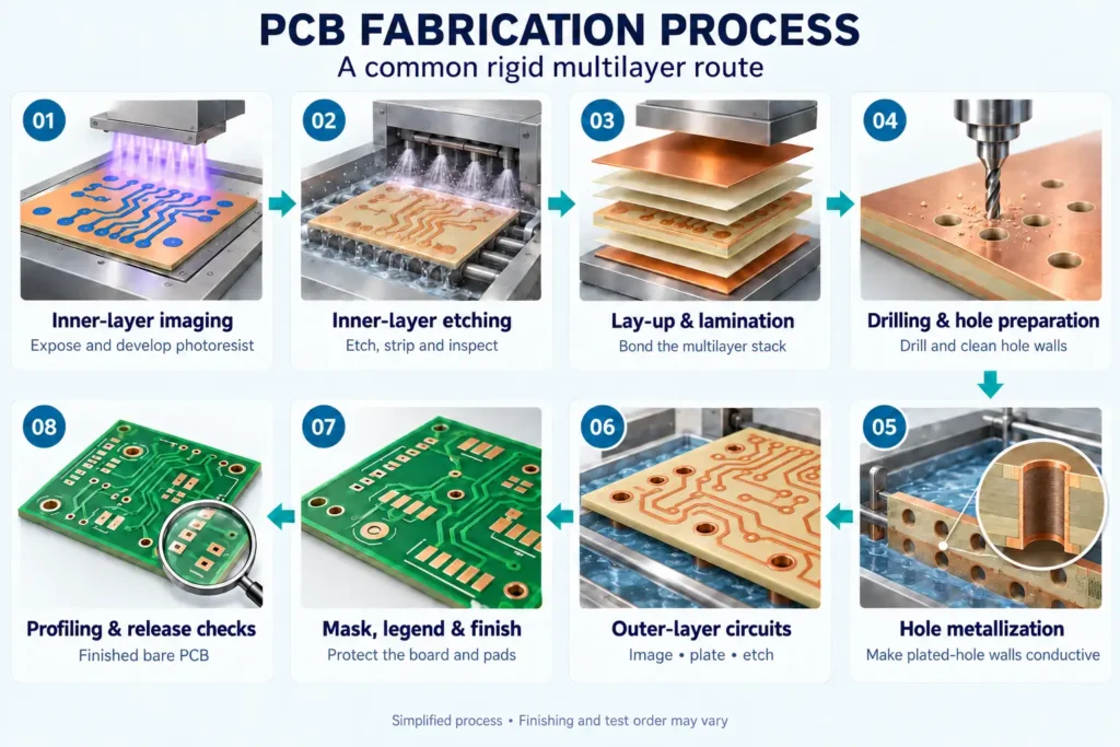
Finishing operations and the order of profiling versus electrical testing can vary. Confirm the actual route when a delivery format or special feature matters.
Imaging and Etching
Imaging transfers a circuit pattern onto a light-sensitive coating called photoresist. For inner layers, exposure and development leave resist over copper that should remain. The areas to be removed are exposed to the etching chemistry.
During inner-layer etching, the process removes unwanted copper. The protective resist is then stripped away. What remains is a copper pattern containing traces, pads, and planes.
Etching must preserve the required conductor widths and spaces. Excess removal can narrow a trace. Incomplete removal can leave an unwanted connection. Automated optical inspection, or AOI, checks the pattern for visible differences before the layers become hidden inside the stack.
For buyers, the useful question is not simply whether a factory uses imaging equipment. Ask how the approved manufacturing pattern relates to your released design. Any proposed change to a critical feature should have a clear approval record.
Outer layers also need imaging, but they are processed later. Their resist pattern serves a different purpose in the pattern-plating route described below.
Layer Lamination for Multilayer Boards
Lamination bonds the layers into one structure. The stack contains patterned cores, bonding sheets called prepreg, and outer copper foil where the construction requires it. Prepreg contains resin that flows and cures during controlled heating and pressure.
The lay-up and bonding process must keep layers aligned while forming the specified thickness. Lamination bonds the stack; copper plating later creates conductive connections through prepared holes.
In a conventional multilayer through-hole route, final through holes are drilled after lamination. HDI and buried-via constructions can require earlier drilling and plating of substructures, followed by further lamination cycles.
Confirm the stack-up before releasing an order. Layer count alone does not define it. The material construction, copper layers, dielectric thicknesses, and finished thickness must match the approved drawing.
Drilling and Copper Plating
Drilling creates holes for interlayer connections, component leads, and mechanical features. Plated and non-plated holes have different purposes. The fabrication data must distinguish them and specify the required finished dimensions. Copper added to a plated hole reduces its opening.
Drilling can leave resin residue on hole walls. Hole preparation, including desmear where required, cleans and conditions those surfaces. For plated holes, the insulating walls need a conductive seed or coating before electrolytic copper can build up.
Electroless copper is one route, but it is not the only one. Atotech’s metallization overview also describes direct metallization processes. The appropriate method depends on the material and manufacturing route.
Next, consider a common outer-layer pattern-plating route. The fabricator applies and develops photoresist so the intended circuit areas remain exposed for plating. This is the distinction shown in outer-layer imaging: resist defines where metal will be added, rather than simply protecting an inner-layer pattern during etching.
Copper plating builds copper on the exposed areas and inside the conductive holes. A temporary tin layer then protects the plated pattern. The remaining photoresist is removed, unwanted base copper is etched away, and the tin is stripped. The outer-layer etching sequence leaves the required circuit pattern.
That temporary tin is an etching resist. It is not the final solderable surface finish. Keeping these operations separate makes PCB etching, drilling, and plating easier to understand.
A practical hole specification should identify finished size, tolerance, and plating status. Do not assume a drill-tool diameter is the same as the finished plated-hole diameter.
Solder Mask and Silkscreen Application
Solder mask is the permanent coating over selected board areas. It differs from temporary photoresist used during circuit formation. Pads and other designated openings remain exposed according to the design.
A typical photoimageable solder mask process includes cleaning, coating, exposure, development, and curing. Inspection looks for misplaced openings, incomplete coverage, or mask remaining on pads that must accept solder.
Silkscreen, also called legend, adds information such as reference designators, polarity marks, and a board identifier. The name does not require traditional screen printing; digital printing can also produce the markings. Legend placement guidance emphasizes keeping markings clear of soldering areas.
Check that essential markings remain readable after manufacturing adjustments. A clipped polarity symbol may cause confusion during assembly. Put the required board revision in the released artwork, and agree on any additional production identification separately.
Surface Finishing
The surface finish protects exposed copper pads and supports solderability. Common options include hot air solder leveling (HASL), electroless nickel immersion gold (ENIG), and organic solderability preservative (OSP).
These treatments have different properties. Surface finish selection should account for component pitch, pad flatness, assembly processes, handling, and storage. There is no single best finish for every board.
Use our PCB surface finish comparison guide to compare the options. Specify the selected finish in the fabrication package. If purchasing receives a proposed alternative, have the assembly team review it before approval.
Surface finishing should not be confused with building copper thickness in traces or hole walls. A board can have correctly formed copper circuits and still need its final pad treatment.
Final Electrical Testing (E-test)
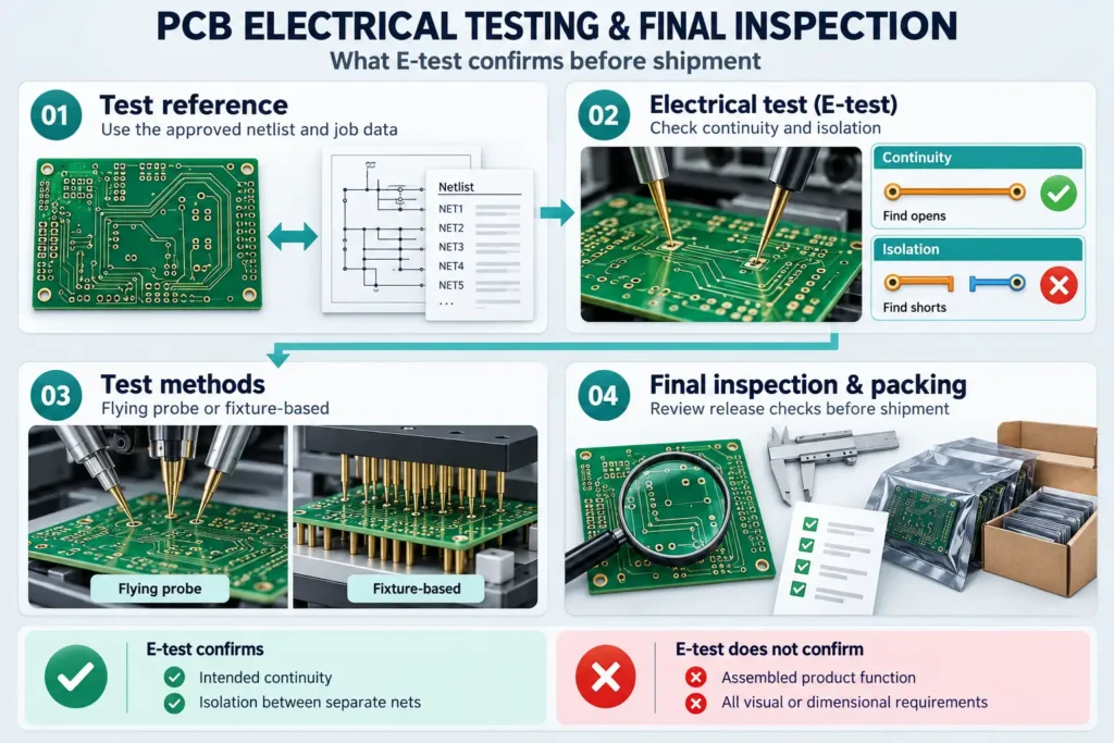
Bare-board electrical testing checks the connection network, or netlist. Continuity testing looks for broken intended connections, commonly called opens. Isolation testing checks for unwanted connections between separate nets, commonly called shorts.
The IPC scope for unpopulated-board electrical testing distinguishes these checks from other physical requirements. Passing an E-test does not prove that the completed electronic product will function. It also does not replace dimensional, visual, or other specified verification.
Flying-probe electrical testing uses moving probes without a dedicated contact fixture. Fixture-based systems use a prepared contact arrangement. Both can test bare boards. The test method, reference data, limits, and reporting requirements should be agreed for the order.
Ask how the test reference is verified. Where available, an independent CAD netlist can be compared with connectivity extracted from manufacturing data. CAD-to-CAM netlist comparison helps check whether those data sets agree. A test based only on the same incorrect artwork cannot independently confirm the original design intent.
Profiling creates the final outline or the agreed delivery panel. Routing and scoring options depend on the design. Electrical testing may occur before or after profiling, according to the production route.
Before release, final inspection brings together the applicable visual, dimensional, and documentation checks. Some checks use sampling; others may cover individual boards. Ask which records will accompany the shipment instead of treating “tested” as a complete acceptance specification.
FAQ
How many steps are in the PCB fabrication process?
There is no universal number. A flowchart may group several operations into one stage. Board construction and the chosen route determine the actual sequence. Multilayer and HDI boards can require additional or repeated operations.
What is the difference between fabrication and assembly?
Fabrication makes the bare board, including its copper circuits, holes, coatings, and finish. Assembly places and solders components onto that board. They require different production files and checks.
What is electrical testing (E-test) checking for?
It checks intended continuity and isolation between separate nets against the specified test reference and limits. It helps detect opens and shorts. It does not test component operation or establish the performance of an assembled product.
Does multilayer fabrication add extra steps compared to single-layer boards?
Yes. Multilayer boards need inner-layer circuit formation, inspection, alignment, and lamination. Certain via structures also require repeated processing. A single-sided board does not need that internal layer stack.
Curious How Your Board Will Be Made?
Explore Benlida’s PCB manufacturing services and discuss the route for your design. Confirm material availability, critical dimensions, inspection coverage, and test requirements for the specific project.
Request a PCB fabrication quote with Gerber or ODB++ files, drill data, and a fabrication drawing. Include the revision, quantity, layer stack, board thickness, copper requirements, surface finish, and any impedance or special acceptance requirements.