

PCB Stack-Up for Signal Integrity — High-Speed Design Rules
What Is Signal Integrity in PCB Stack-Up?
A PCB stack-up for signal integrity places critical signal layers beside continuous reference planes. It controls trace geometry and dielectric spacing, while giving return current a clear path through layer transitions. These choices help limit reflections, unwanted coupling, and electromagnetic interference. They do not replace correct termination, routing, or system testing.
Signal integrity means that a receiver sees the intended signal with enough voltage and timing margin. The stack-up defines the copper layers and insulating materials through which that signal travels. A trace and its reference plane form a transmission structure, not two independent pieces of copper.
Start with edge speed, not clock frequency alone. TI’s high-speed layout guidance explains how rise and fall times affect the higher-frequency content of digital signals. Even a modest clock can have fast edges. Trace length, driver behavior, and receiver requirements determine whether those edges need transmission-line treatment.
This guide focuses on how layer choices affect electrical behavior. For construction terminology and the wider planning process, see the PCB stack-up design guide.
Reference Plane Placement Rules
Identify the reference plane or planes for each critical routing layer before routing begins. For high-frequency signal content, return current tends to concentrate near the trace on the reference plane. A slot, split, or large void can force that current to detour. The resulting loop can increase inductance and interference.
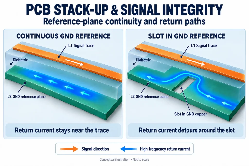
Inspect the whole route, including connector escapes and dense via fields. A ground layer can look continuous in the stack drawing yet contain a barrier made by overlapping via clearances. Do not route across that barrier simply because the layer is named GND.
When a trace changes layers, check whether its reference changes too. If both routing layers share one continuous ground plane, the return-path problem differs from a transition between separate ground planes. For the latter, TI’s interface layout guidelines show ground stitching vias near the signal transition. Their job is to connect the relevant ground references locally.
A power plane can also serve as a reference. However, its splits, noise, and connection to the rest of the return path need review. Altera’s power and ground layer guidance favors ground references when there is a choice. It also warns about coupling switching noise into sensitive power rails.
Never connect power and ground with a stitching via. A transition between different reference nets may need an engineered AC return path. A nearby capacitor is not a universal fix: its mounting inductance and effective frequency range matter. Prefer a route that avoids unnecessary reference changes, then review unavoidable transitions with the hardware or SI engineer.
Layer Ordering for High-Speed Signals
Plan the signal integrity layer stack around the critical routes first. Identify the interfaces, connector positions, package escapes, and power rails. Then reserve suitable layers for those routes. Filling every available layer with signals can leave too few continuous references.
Outer-layer microstrip and internal stripline offer different trade-offs. Microstrip may avoid vias between surface-mounted parts. Stripline places a signal inside the dielectric between reference planes. Neither is automatically the best choice for every interface. An internal signal can couple to both bounding planes, so its model must include the actual construction.
Layer order alone is incomplete. Record dielectric thicknesses, copper thicknesses, and material construction alongside the layer functions. Agree on a mechanically balanced build with the fabricator. Adding layers creates options; it does not guarantee that the chosen routes use those options well.
Use the following rules as a review checklist, not as fixed manufacturing dimensions.
Stack-Up Rule Table
| Design Rule | Purpose | Typical Implementation |
|---|---|---|
| Provide continuous references | Keep the return path close to the signal. | Check planes beneath complete routes, including via and connector areas. |
| Plan reference transitions | Limit return-current detours at layer changes. | Connect relevant ground planes near signal vias; review different-net references separately. |
| Define each transmission structure | Keep impedance calculations tied to the build. | Specify routing layer, reference planes, dielectric spacing, copper, width, and pair gap. |
| Separate coupled routes | Reduce unwanted signal-to-signal coupling. | Place a continuous reference plane between sensitive routing layers where practical; review spacing and parallel run length. |
| Review power distribution | Support the supply network without breaking signal references. | Locate power regions and decoupling paths before assigning nearby critical routes. |
| Approve the finished construction | Prevent unreviewed changes after routing. | Recheck geometry when materials, dielectric thickness, or copper requirements change. |
Impedance Control Through Stack-Up Design
An impedance-controlled stack-up describes a transmission structure on each controlled layer. Trace width is only one input. Dielectric spacing, material properties, finished copper thickness, trace shape, and differential-pair gap also affect the result.
Use the fabricator’s proposed pressed construction, not an assumed board thickness divided equally among layers. Request the material grade and dielectric data appropriate to the design frequency and modeling method. FR-4 is a material family, not one universal dielectric constant.
On outer layers, include solder mask where present. Polar’s solder-mask modeling note shows why the coating profile belongs in a coated-microstrip model. Evaluate manufacturing variation rather than treating the nominal calculation as the entire acceptance window.
Impedance is also separate from channel loss. A route can meet its impedance target yet lose too much signal over its full length. Rogers’ material guidance discusses how copper roughness affects loss and phase behavior. Choose material and copper using the channel budget; do not assume a specialty laminate repairs a broken return path.
Specify targets and tolerances by interface and layer. Confirm them against the selected device documentation. The PCB impedance control guide covers ordering details and verification. A passing impedance coupon supports fabrication control; it does not validate the complete assembled channel.
Minimizing Crosstalk Between Adjacent Layers
Crosstalk occurs when one signal couples unwanted energy into another. Coupling occurs between nearby traces on one layer and across adjacent signal layers.
For two adjacent internal signal layers, review both their separation and their distances from the reference planes. Altera’s crosstalk guidance combines perpendicular routing with greater signal-layer separation and closer reference planes. Perpendicular routing reduces extended overlap, but it is not a substitute for suitable geometry.
Keep unrelated fast nets apart and shorten their parallel runs. When practical, separate sensitive routing layers with a continuous reference plane. Distinguish the gap within a differential pair from the clearance between that pair and other nets. Increasing one changes a different electrical relationship from increasing the other.
Spacing rules based only on trace width cannot certify every design. Use the actual stack-up, coupled length, edge rate, and receiver noise budget to set constraints. Check dense escape areas and length-tuning sections, where spacing may shrink. Validate critical channels through suitable simulation and measurements.
For boards that also carry RF paths, the high frequency PCB design guide covers the additional material and routing considerations.
Stack-Up Examples for Common High-Speed Interfaces
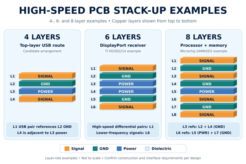
These examples explain layer roles. They are not ready-to-release stack-ups or promises that a given layer count will pass an interface test. Sequences run from top to bottom. S means signal, G means ground, and P means power.
Four Layers for a Top-Layer USB Route
A candidate arrangement is S / G / P / S. Route the critical top-layer pair over the continuous L2 ground plane. The bottom layer sits next to power, so moving the pair there changes its reference environment. Do not treat both outer layers as electrically interchangeable.
TI’s USB layout training discusses solid references and routing priority for USB layouts. Apply the selected controller’s rules for the USB generation in use. If connector placement forces awkward transitions, reconsider placement or layer count before adding more vias.
Six Layers in a DisplayPort Receiver Example
The TI HD3SS214 data sheet shows S / G / P / P / G / S for a receiver-board example. High-speed differential traces occupy L1, while the bottom carries lower-frequency single-ended traces. The inner layers provide two power regions and adjacent ground planes.
This arrangement adds power-distribution space without adding internal signal-routing layers. It can therefore be unsuitable for a dense memory breakout. The lesson is to count usable routing layers, not just total copper layers.
Eight Layers for a Processor and Memory Board
Microchip’s SAMA5D2 design guide includes S / G / S / G / P / S / G / S. Its impedance table identifies two references for L3: L2 and L4. L6 references L5 and L7, so the power layer remains part of that structure.
For DDR routing, follow the specific controller’s topology, delay, and matching requirements. Equal physical lengths on different structures need not mean equal delay. Extra routing layers help only when escape routing, reference continuity, and power distribution are planned together.
Before approving a stack-up, trace one complete critical connection from driver to receiver. Mark its routing layers, reference planes, vias, connector transitions, and termination. Then repeat the check for the other interface groups. This makes hidden reference changes easier to find. If the fabricator proposes a construction change, update the routing constraints and electrical model before approving it.
FAQ
What is the biggest signal integrity risk in PCB stack-up design?
There is no universal ranking. A broken return path is a serious risk because it can create impedance changes, coupling, and emissions. Wrong geometry, excessive loss, and poor termination can also dominate. Review the complete route and its references rather than judging the layer drawing alone.
How many layers are typically needed for controlled impedance?
Controlled impedance is possible on a two-layer board with a suitable transmission structure. Four or more layers often make continuous references and routing easier to arrange. Dense processors or memory interfaces may need more. Select the count from routing, power, mechanical, and electrical requirements, not impedance alone.
Does reference plane placement affect EMI performance?
Yes. Reference placement influences return-current paths and loop area. Continuous nearby references and well-designed transitions can reduce unwanted radiation. They do not guarantee EMC compliance: connectors, cables, power distribution, enclosure design, and other circuits also affect the finished product.
Can Benlida validate my stack-up before manufacturing?
Ask Benlida to review the proposed construction and confirm the available engineering scope for your project. Separate manufacturability and impedance verification from system-level SI analysis. If you need channel simulation, eye-diagram evaluation, or compliance testing, agree on responsibility and deliverables before placing the order.
Designing a High-Speed Board?
Explore Benlida’s multilayer PCB manufacturing service. Request a stack-up review for your specific design.
Send the proposed layer sequence, board thickness, materials, copper requirements, and impedance table. Include Gerber or ODB++ data, drill files, fabrication drawings, quantity, and revision. Identify critical interfaces, reference planes, and any required via-stub controls.
Confirm the approved construction and review scope before production. Keep system-level electrical validation as an explicit project requirement.